WEEK 6
Electric Design
Assignment:
- Redraw the echo-hello-world board, add (at least) a button and LED (with current-limiting resistor), check design rules, make it (if you have time this week, test it).
Option: simulate its operation. Measure its operation.
Software(s):
- EAGLE
- Adobe Illustrator
Skill(s):
- Circuit Design
- Soldering
- Programming
- Milling
SCHEMATIC DESIGN
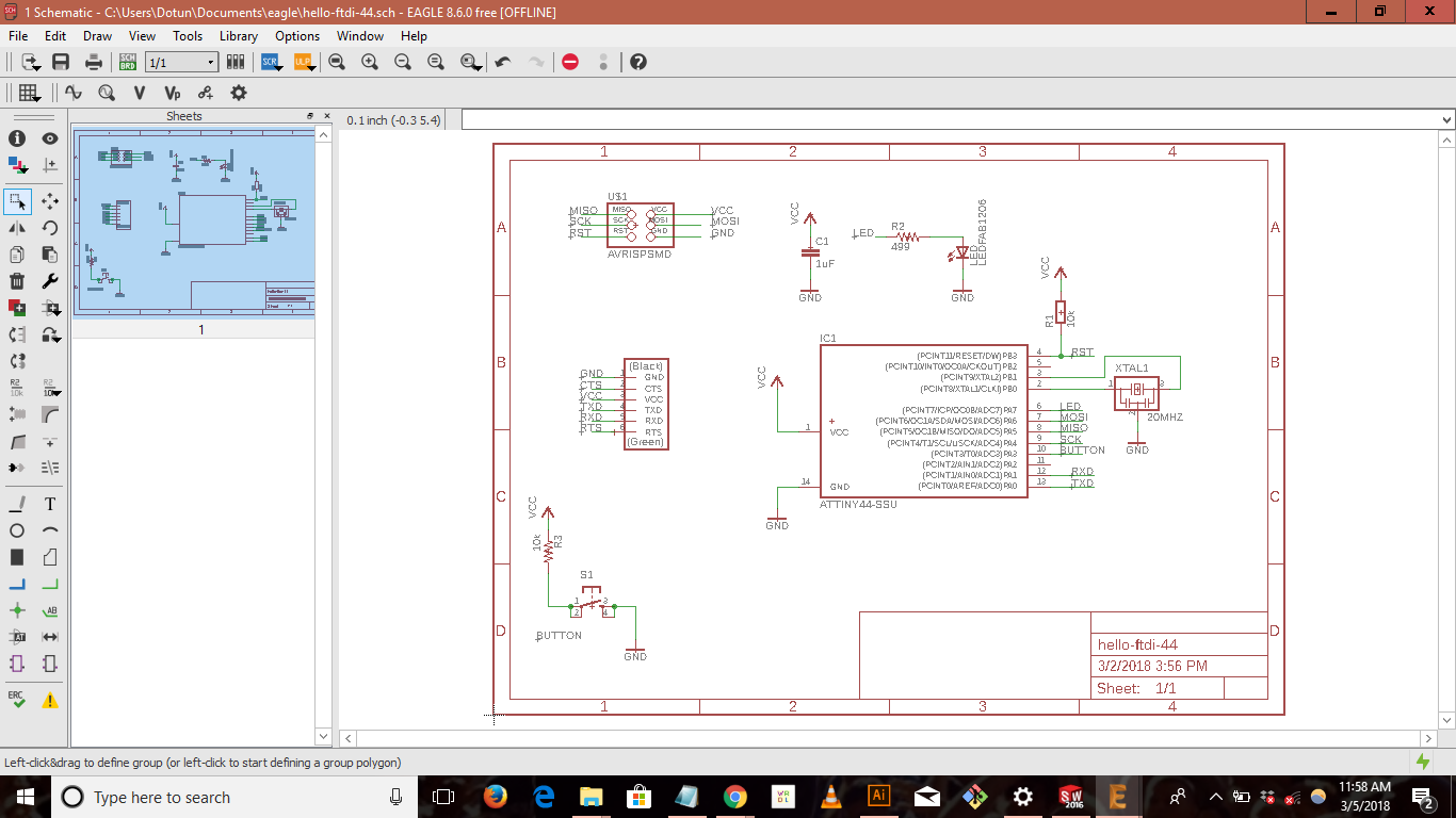
This will be the first time using EAGLE or any circuit designing software. At first glance EAGLE was intimidating but after a few uses the UI was easy to navigate and pretty straight forward. Following Fab Academy’s tutorial, Introduction to EAGLE (http://docs.academany.org/FabAcademy-Tutorials/_book/en/week6_electronic_design/eagle_english.html) was very helpful. To get myself up and running, I had to first download and install Eagle onto my laptop. As Eagle was installing I downloaded the example schematic file “hell.fdti.44 schematic” file from the tutorial. With all the files downloaded, I was officially ready to start creating my board. First step was to create the schematics of the board. With the example file open in EAGLE is was able to follow the steps demonstrated in the tutorial. This step was pretty straight forward but I did run into some learning curves regarding EAGLES schematic design interface. It took me some time getting use to the connecting components via naming but once I realized you have to net, name and label the components, it was smooth sailing.
LAYOUT DESIGN
My experience with EAGLE’s layout design mode was a little different. The learner curve for my was slightly larger than the once for Schematic mode. Following the tutorial mentioned above was very helpful for this stage. Once I got a hang of the layout design user interface, I was able to complete my board. I made some design change to the board because I didn’t want to completely copy the board from the tutorial. (Quick Note: EAGLE’s Auto Routing feature is not the greatest. Initially I used auto tracing as instructed in the tutorial but the results were subpar. The Auto Routing feature created a few traces that overlapped each other. I ended up having to cut and re rout majority of my traces after using Auto Routing. I think AutoRouting is a great tool to start with as it gives you an visual idea of what need to be connected to what but once you become fluent in EAGLE manually routing traces seems to be the more efficient method.)
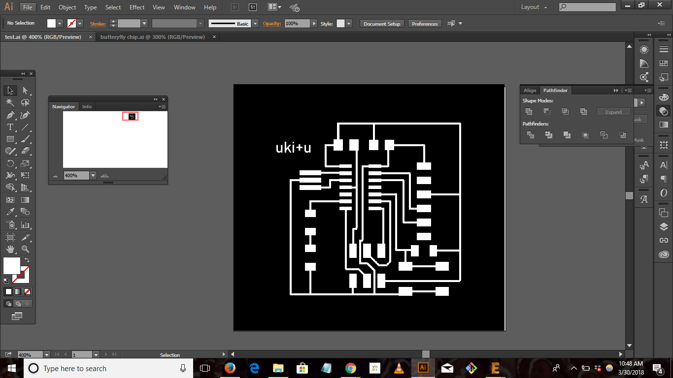
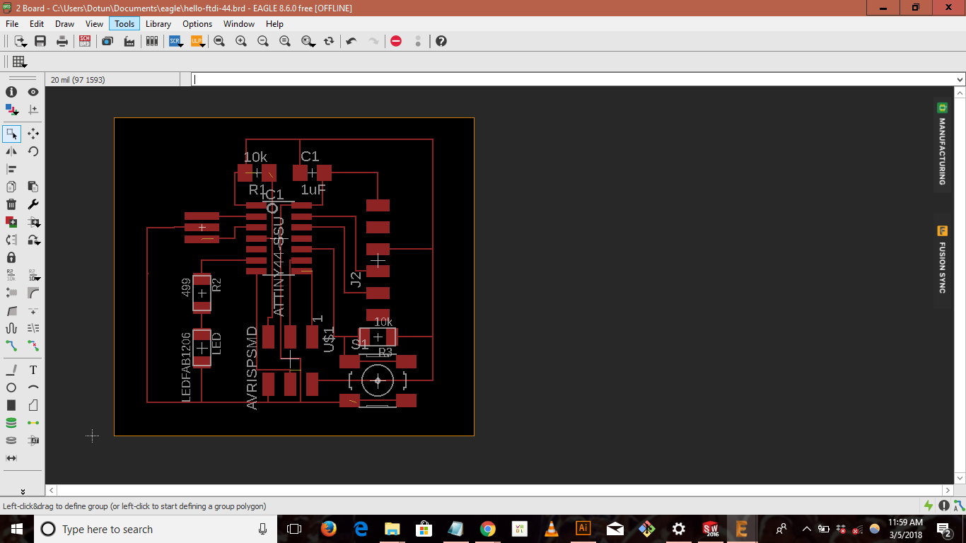 With my schematic and layout designs complete, the next step is to export my board. A helpful trick I used when exporting layout design was to decrease the size of the “orange” boundary box to surrounding your circuit layout. This allowed me to skip the cropping step since when exporting the boar you have the option to export only what is within the boundary box. At this point I deviated from the tutorial and used Adobe Illustrator to clean up my exported board and get is ready for milling. The difference in Illustrator is that when you upload the layout file, depending on you default settings your “artboard” will be much bigger than the file. A quick fix to this is going to preffences > edit art board and decreasing the artboard to surround the export file. Once this is done any edits can be made to the board. At this point I decided to add “ukitu” to the top left of the board.
MILLING & SOLDERING
Similar to week 4’s assignment, I used a combination of Mods and the Roland to mill my board.
PROGRAMMING
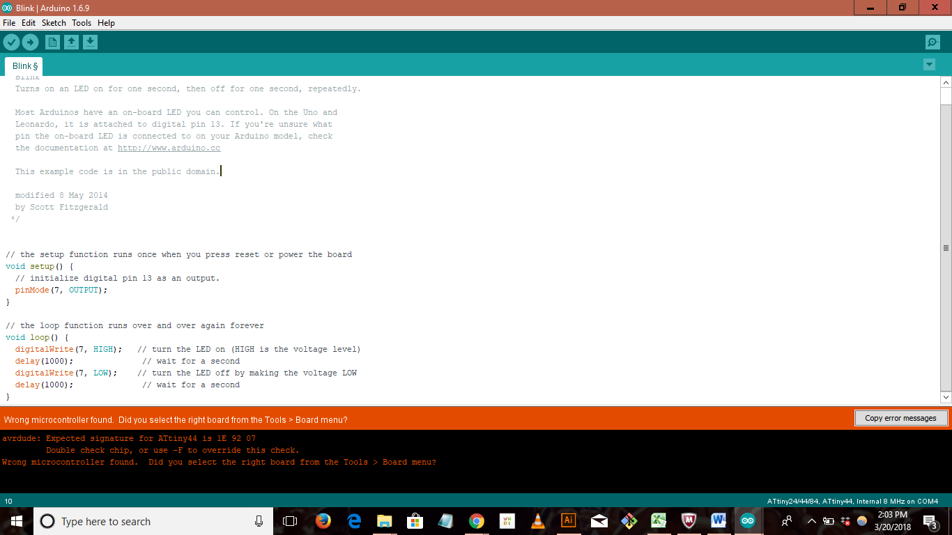
I ran into a few road blocks when it came to programming the board. For my programmer I was using my Arduino as an ISP. Following this tutorial (http://www.instructables.com/id/Turn-Your-Arduino-Into-an-ISP/) the first step I took was to run the “ARDUINO AS ISP” sketch onto my UNO. This sketch enables the Arduino to act as an ISP. Uploading the sketch was pretty quick. The next step was downloading the correct IDE for ATTINYs into the board manager and downloading the files. Once files are download, I made sure my settings were correct, tools = attiny44, clock=20hmz etc and tried to burn the bootloader. This is where I started running into problems. I started receiving “expect signature” errors when trying to upload a simple blink code to my board. At this point I started troubleshooting my board and set up.
TROUBLESHOOTING
- Check for short circuits – Using the multi-meter and visual inspections I searched for any sign of faulty wiring. Everything seemed good with the board. I did notice that my “traces” were pretty thin. I thought this may be a problem. There might potentially be a trace that I ripped up without knowing.
- 2. Check Arduino and connection – The connections seemed to correct. I followed the mentioned above and tripled checked my board setup.
After going through my troubleshooting steps, I decided to make a new board. The first board I made did not work and Im not too sure why. I tried troubleshooting the problem with a visual inspection and voltmeter but no luck. After a while to save time I decided it would be better to make a new board. Plus I will be getting more experience using the Roland.
The second board ended up being a bust as well. Initially the board looked great. Milling and stuffing the board were smooth. When I tried to burn the bootloader I Kept receiving “incorrect signature” error messages. After a few tries I started my troubleshooting process. First voltmeter, visual inspection and connection check. After intense inspection I found the problem. Not sure when it happened but one of my traces were ripped apart from my board. Luciano and I tried repairing the traces by soldering a piece away to connect the traces where the rip happened but that didn’t seem to work. On to the next one.
The third board was the final onr. Milling and stuffing went well. After each process I did an intense visual inspection of the board to make sure nothing was missing, ripped or corrupt. Once the board was stuffed I was ready to program it. First I burned the bootloader, and then uploaded a simple blink sketch to my board. Boom my board works!
const int button = 3;
const int led = 7;

// the setup function runs once when you press reset or power the board
void setup() {
  // initialize digital pin 7 as an output.
  // initialize digital pin 3 as an input.
  pinMode(7, OUTPUT);
  pinMode(3,INPUT)
}

// the loop function runs over and over again forever
void loop() {

  buttonState = digitalRead(button);
  if(buttonState == LOW) {
    digitalWrite(7,LOW);
  }

 else(buttonState == HIGH) {
  digitalWrite(7,HIGH);
  delay(500);
  digitalWrite(7,LOW);
  delay(500);
  digitalWrite(7,HIGH);
  delay(500);
  digitalWrite(7,LOW);
  delay(500);
 }
   delay(1000);              // wait for a second
}
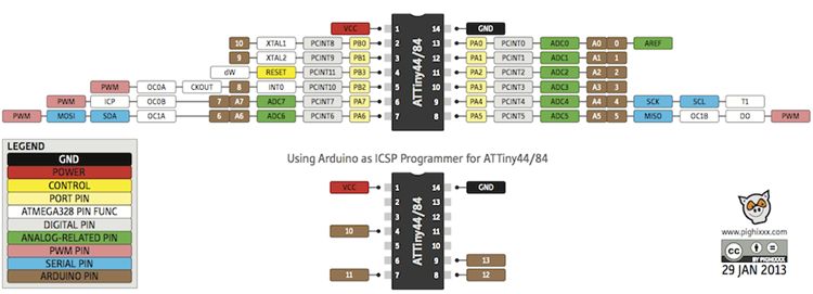
(QUICK NOTE: If you look closely and compare the LED pin out on the hardware and code you will see that they do not match. The LED pin on the board is connected to pin 6 on the Attiny44 but in the code the LED pin is 7. For some reason, that I’m not too sure about, the pin mapping changes when using Arduino. Google was my friend in this case. I found good rendered mapping of Atrtiny44 Arduino pinouts via google searching. Pic of Attiny44 Arduino Pin Out)
BUTTERFLY BOARD
After completing the assignment I had some free time and wanted play around with my board design. I remember NEIL mentioning a past Fab Academy student that designed a board by hand and was inspired to make something cool.
The first step was designing the board and layout. I this by hand, for me sketching concepts by hand gives me a better feel of the design. This was especially helpful for this project because the design and layout process was quite difficult. The shape of a butterfly is not necessarily the most space efficient shape. When figuring out the layout of the components I realized that both orientation and positioning are very important. After a few sketches I was able to figure out the perfect layout for my board.
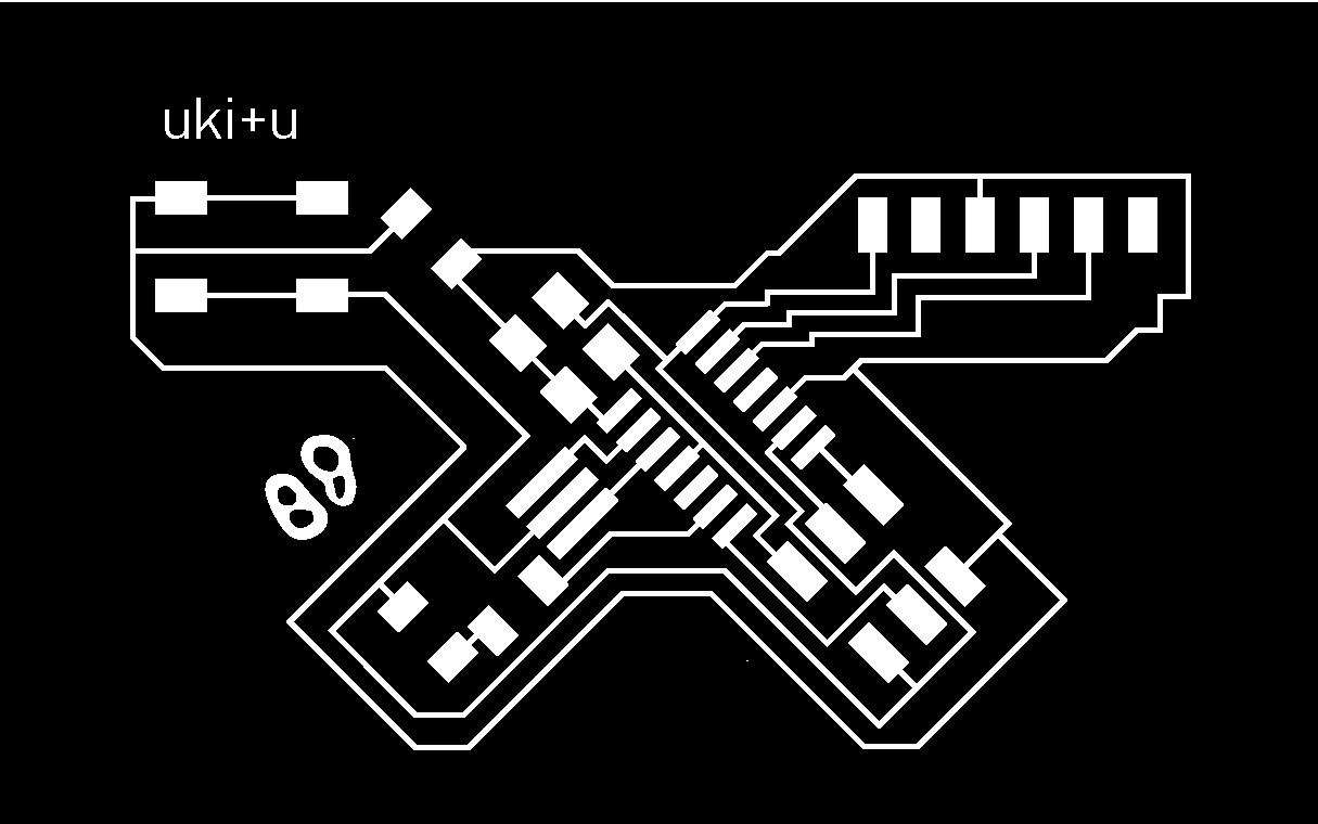
Next step was creating the traces and shape png files. For this step I decided to skip EAGLE and go directly into Adobe Illustrator. My reasoning for this is because I have better control of Illustrator than EAGLE. Plus I’m not certain you can make such unique shapes with EAGLE. The first thing I did in Illustrator was find a picture of a butterfly that I like. Once I found the picture I imported the picture into Illustrator and used the image trace tool. When using image trace, the presets can be adjusted to achieve your desired outcome and level of detail. For me since I just wanted the outline of the butterfly I used the “3 colors” present and expanded the image which turns the image to editable vectors. This outline will serve as the boundary and cutting shape of my board.
 This will serve as the shape of my board. The next step is to fill the inside of the butterfly but first I had to figure out how to recreate each component in illustrator. For this I used the same technique used to create the butterfly outline. I used the Hello-Board I exported from EAGLE since the board had all the necessary components for my new board. I imported the Hell-Board png file in illustrator, image traced and expanded the png. This left me with Vectors of the traces and png. With these vectors I was able to create accurate copies of each component.
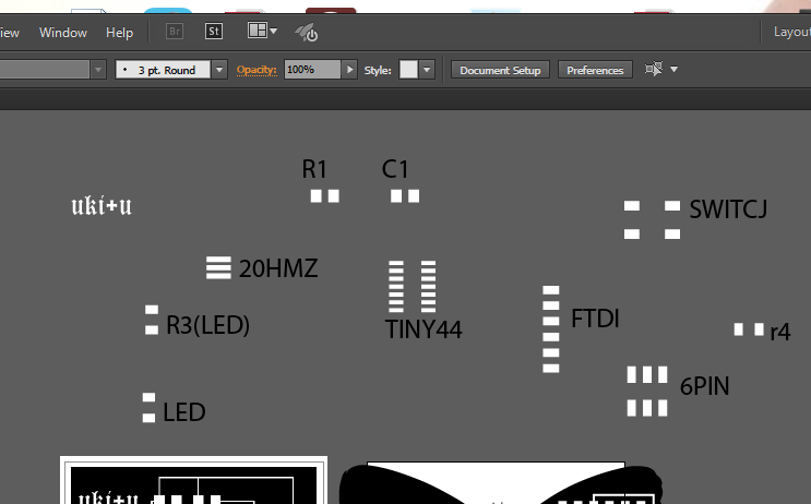 Following my sketch I placed each component based on the layout I designed. I added a few signature design aspects to my board and exported the Traces and PNG file of my board.
MILLING
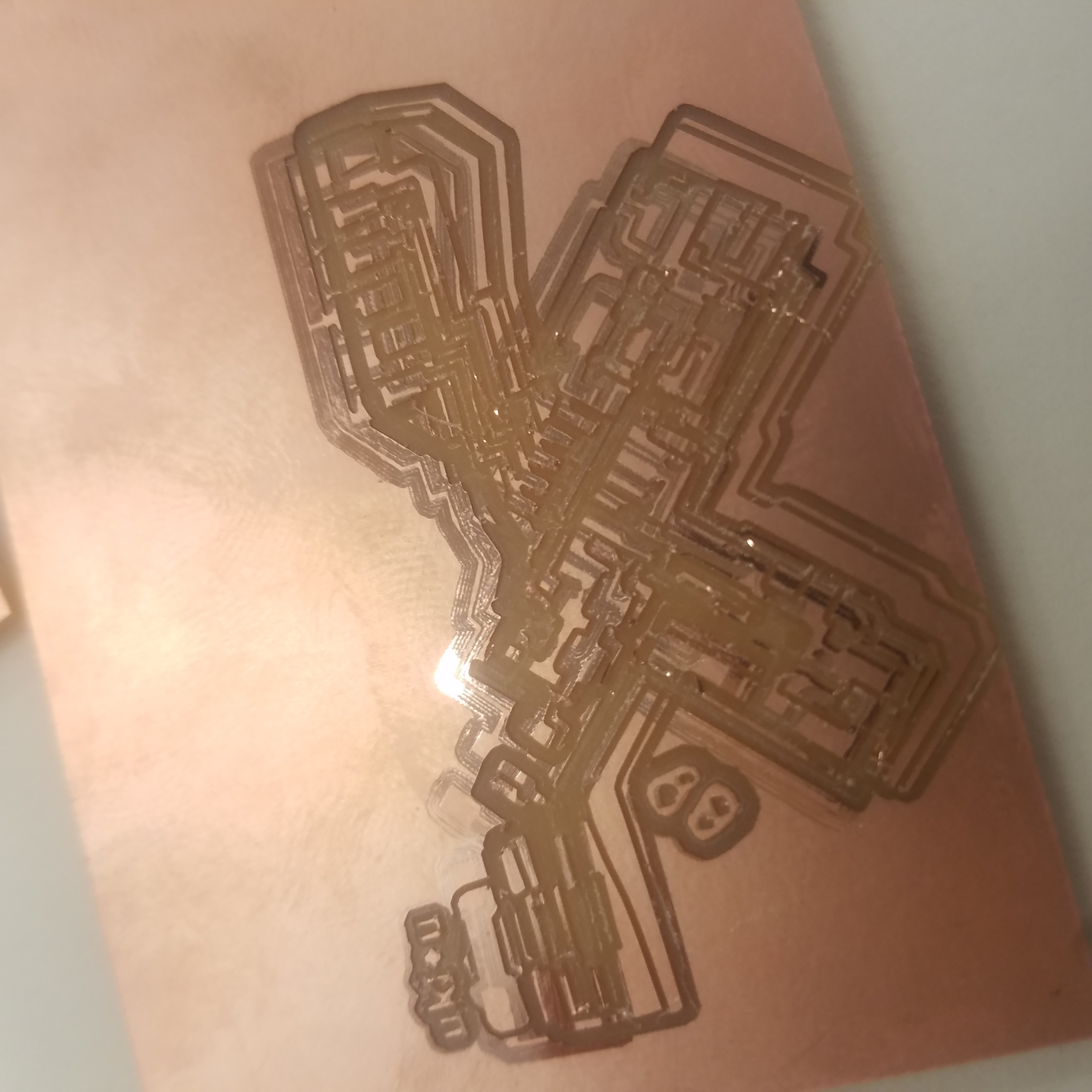
Compared to designing the board the difficulty level of milling of this board was almost side by side. I ran into several problems when I tried to mill my board, ripped traces, crooked lines, uneven milling etc. There were a lot of trial and error but after 7 failed board I was finally able successfully make my board.
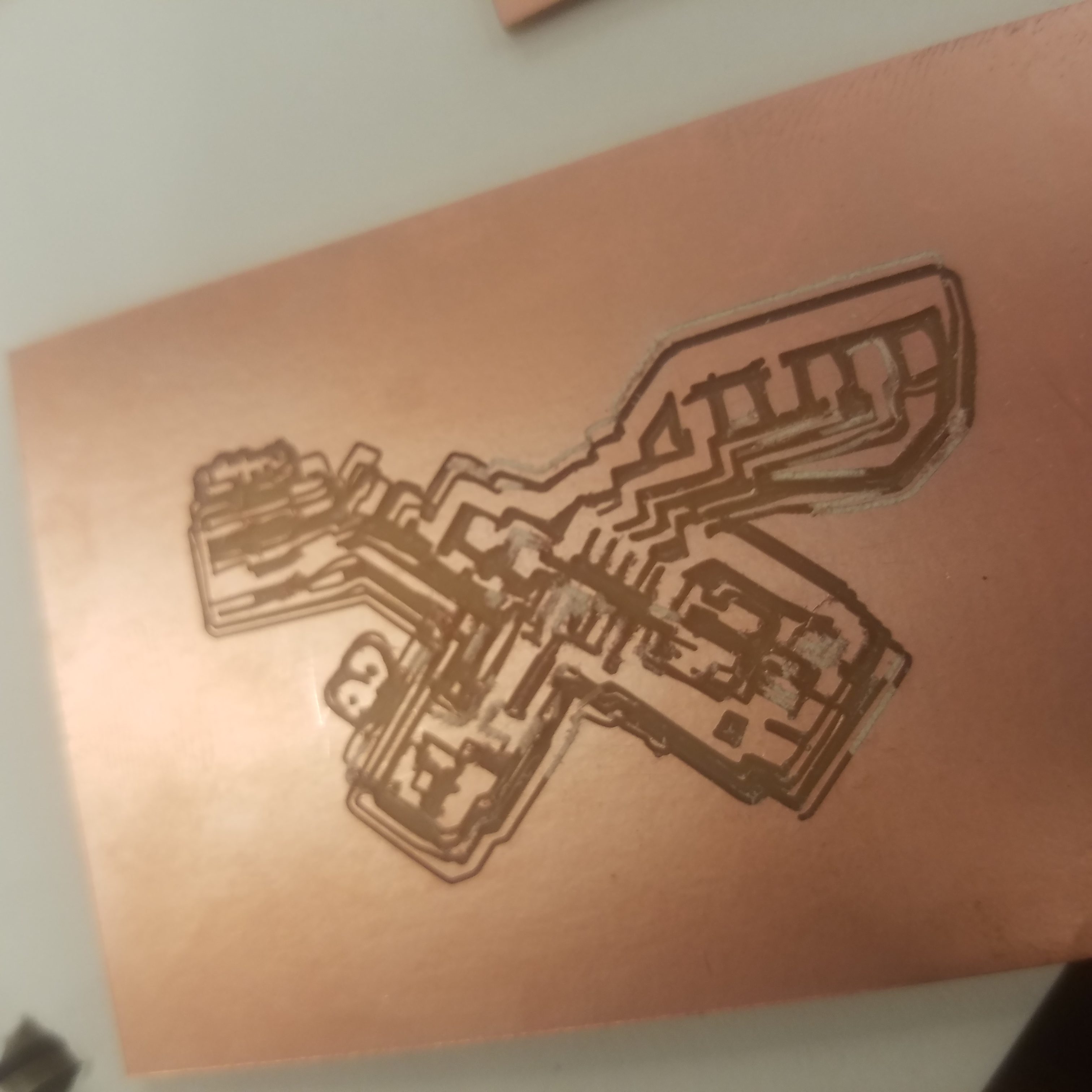
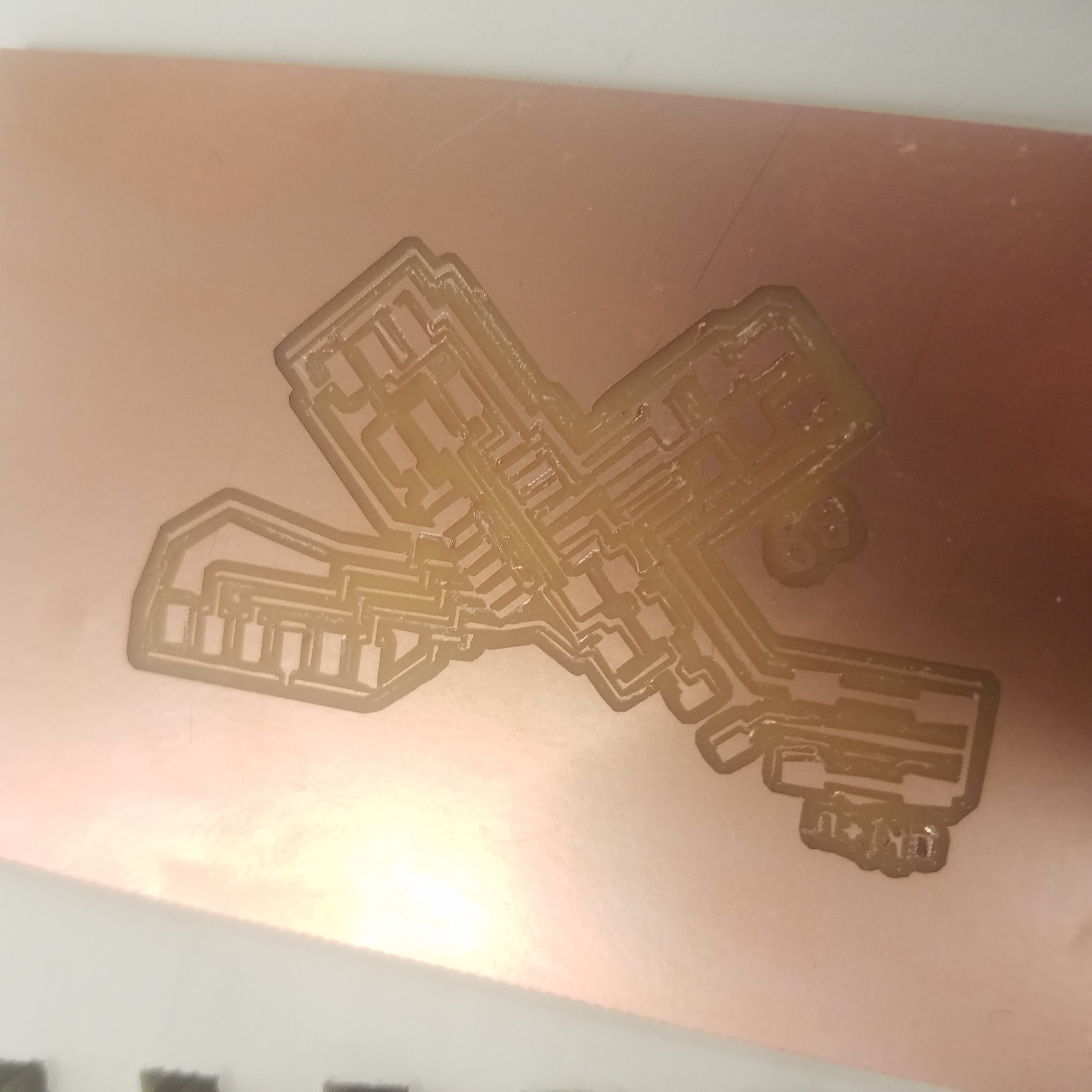
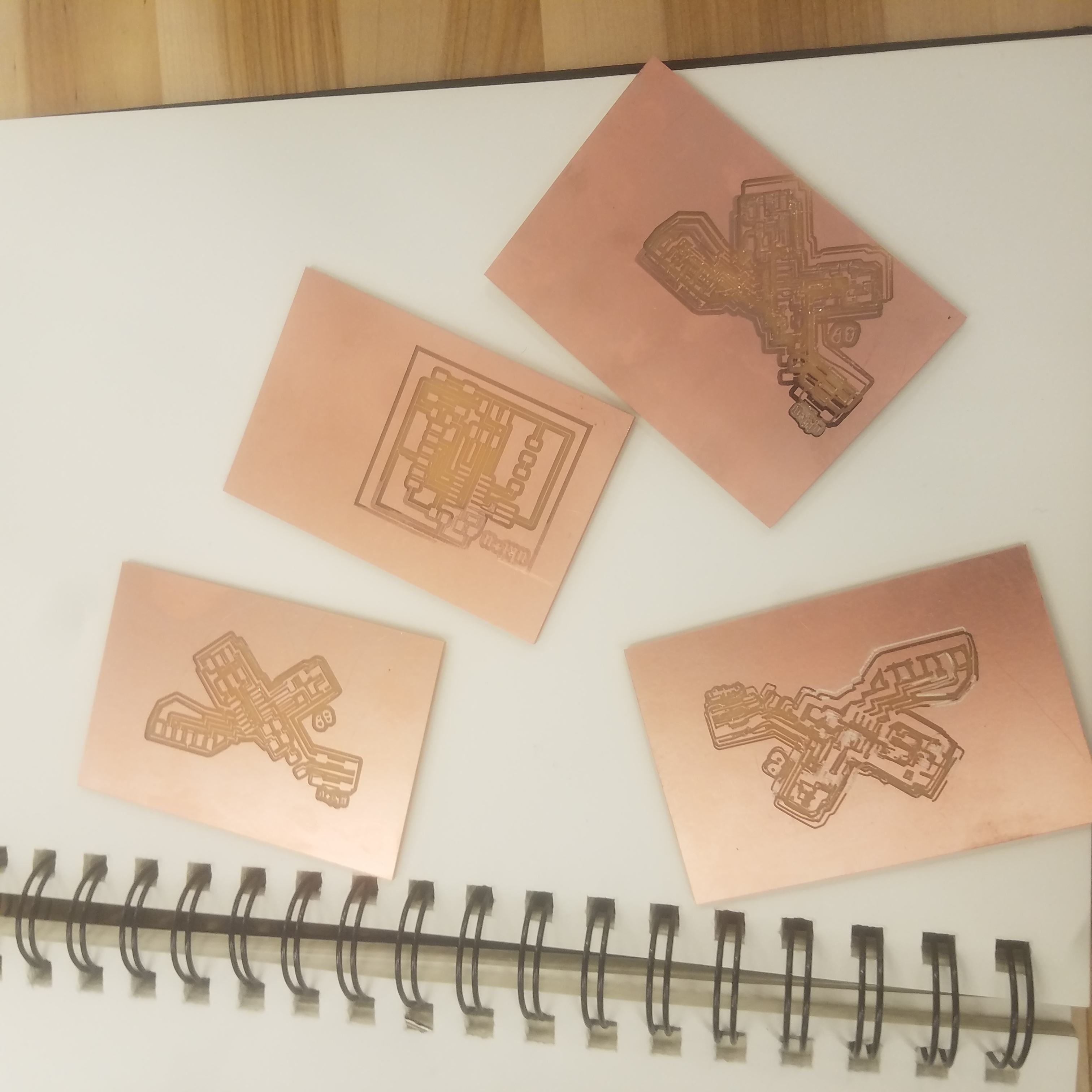
Here are some of my takeaways:
- The Roland SRM-20/MOD does not do will with angled lines that are not at a 45 degree angle. My initial design had lines with a variety of angles and the ones that were not at 45 degree came out pretty bad. My theory is that this is correlated to the capabilities of the motors. When a line is at a 45 degree angle the Roland produces a straight line but when the line is plus or minus 45 degrees the Roland produces “steps” instead of a straight line
- A good with for routs is 0.007”. When I tried to go smaller than this my traces would rip apart during the milling process.
- MOD settings
Offset: 1
Threshold: 0
Threshhold: 0
Depth: 0.006
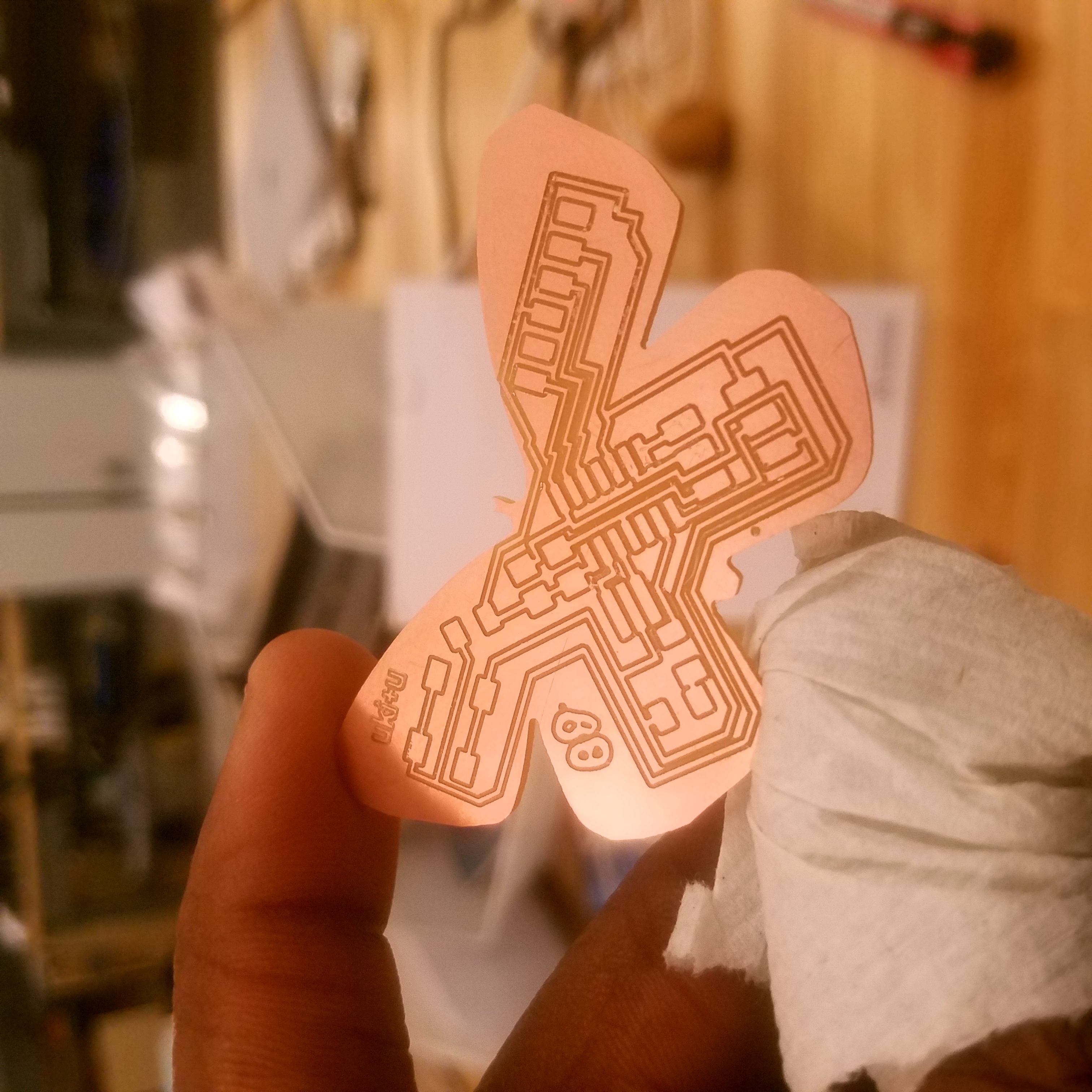
I ended up not stuffing the board. After finally creating the board I was too happy with how it looked and didn’t want to ruin it haha
FILES:
Butterfly Traces
Butterfly Shape Outline
Echo Hello-World w/ Button & LED
Echo Hello-World Shape