Week - 05 Electronic Production

Group work of this week is about characterization of machine in which we all learn about pcb milling machine , milling bits , smd components and mill 3-4 pcb boards in group and individually also , we all are new to this process so we refer previous year work of our mentor Rudrapalsinh Solanki work 2016 and gautam prakesh work 2017 fab acadmy student and see tutorials of pcb milling.
Things we all learn
a Introduction to pcb
b Introduction to milling machine Roland models mdx-20 and operations
c Introduction to milling bits
Introduction to pcb
A printed circuit board (PCB) mechanically supports and electrically connects electronic components using conductive tracks, pads and Components (e.g. capacitors, resistors or active devices) are generally soldered on the PCB, it can be of single-sided (one copper layer), double-sided (two copper layers on both sides of one substrate layer), or multi-layer (outer and inner layers of copper, alternating with layers of substrate
We have zero pcb and fr4 pcb boards in our lab which are single sided and double sided we used single sided board in which FR-4 It is a composite material composed of woven fiberglass cloth with an epoxy resin binder that is flame resistant (self-extinguishing) and FR-1 is a hard, flat material that consists of a thin layer of copper over a non-conductive phenolic resin
We use FR1 even thou they are not as strong as the FR4 and bit mills nicely and the end mill lasts longer and also fR4 when milled produces glass fiber shreds which can be dangerous if inhaled, although they can sustain higher temperature
Introduction to PCB milling machine
we have roland models mdx-20 pcb milling machine in our lab we first try milling , It is a tiny desktop CNC that can mill PCBs, create 3D models on wax it has a small bed which moves in the Y-axis, a Tool head which moves in the X-axis and the end effector which moves in the Z-axis. It supports many milling bits and is easy to use.


Introduction to milling bits
tracing bits
1/64 inch SE 2FL bit of carbide bits and 1/64 inch garr tool bit we use for tracing operation
Cutting bits
we are using 1/16 bit for cutting operation as we are missing with 1/32 bit so we used 1/16 bit we changed the bit dia to 0.4 in cutting setting


Process of milling on Pcb milling machine
FAB MODULES:
FAB Modules is used to run Roland Modela MDX-20
To begin with, Open Terminal Window on Ubuntu OS by pressing “Ctrl+Alt+T” and Write “sudo fab” and hit Enter, then Fab Module page will get opened in that select respective things as follows:
Input Format : .png
Output Format: Roland MDX-20 mill (.rml)
Now Click “make_png_rml”
Select Mill trace as 1/64 and click on load .png.
Now, make path – change the x(min) and y(min) position according to the space where the circuit is to be milled – and click on Move to x(min) and y(min) button – make .rml – make path – again make .rml – send it
Step 1: First you have to measure the thickness of your board before
Start milling as you need this parameter while assigning cutting depth
Step 2 : Setting up pcb on bed
Take the double sided tape and put on that board and stick that board on the bed of modela and tight the bed equally all side.


While applying tape note that there should not be any air gap and no overlapping of tap as it will create uneven surface level
left -top corner of your bed on viewing from front is the origin set point of your machine . fix your pcb here and make sure that there is no air gap between bed and pcb
Step 3 : Setting tool
We are going to set first1/64 inch milling bit in spindle for milling we set the bit using Allen key.
This is setting the tool at home position in this hold the tool while fixing
otherwise if it fall down your bit will be get broken

Setting again tool before start milling as while setting tool above pcb you have to loose tool and let the tool drop down by gravity carefully so the bit wiill not get broken and fix the tool here

Step 4 - Load your file and generate rml file to begin milling
you have to install first fab module in your Linux system to begin milling as here is guide to it installation guide
for group work we all together mill fab lab cept isp which is designed by our mentor rudhra

As we kept here offset 1.5, zmin to 0.15 so our bit is broken and error to 1.1


We have changed our parameter to offset 2 and zmin to -.08 and mill another board

Make rml file and click on send it button so machine will start tracing

at this stage your milling work of tracing your board is done

Again change the bit now fit 1/32 inch bit and set again the origin as previous point

Now load png file for cutting process and make path and make rml file

Now begin milling for running cutting path

Now remove the board carefully

Now remove the tap and take your board out

Our board is milled properly , for checking you may also use multimeter

Assignment work for characterization of machine is done

Line Test
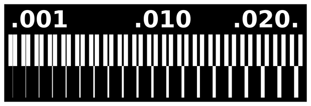
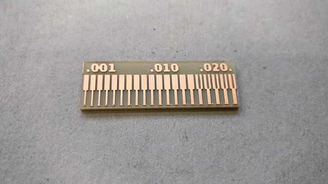
Through the group assignment, we will go through the process of fabricating a Traces-width board, assessing how separated can our traces be, as well as how thin they could potentially be. The board we will be machining is found below, and we will be using copper PCBs machined in either Modela MDX-20.
The traces png file to be machined with a 1/64” tool:

To cut the board out of the copper layer, we will use a 1/32” tool on the following profile:

Both png files will be passed through the FabModules. Note that this tool will detect changes between BLACK and WHITE in the png files and generate a path in it for the machining process.
The settings selected for the PCB traces are:
●Upload image as *.png
●Output file as Roland mill (*.rml)
●PCB traces (1/64)
●Machine: MDX-20
●Origin: X10, Y10 and Z-0.01 are set ,you can set as per your placement of pcb
●ZJog is set to 2mm, meaning that the machine will lift the tool 2mm while not cutting
●Xhome, Yhome, Zhome are set to 0mm, 0mm and 5mm. The latter being the most important, since it is the value at which the tool will be positioned once the job is finished. If this value it’s zero, it will scratch the whole copper surface, very likely breaking the tool
●Cut depth: 0.19mm
●Offset: -1. It’s the number of offsets that the program will calculate out of the BLACK-WHITE transitions. A number of -1 will remove all the copper.
●Offset-overlap: 50%, relative to the tools diameter (1/64” in this case)
The settings selected for the PCB outline (only detailing the ones that are different):
●Cut Depth: 0.4m
●Stock thickness: 1.5mm
●Number of offsets: 1


Somehow the fab modules was not able to detect the lines beyond a certain dimension. The changes were very minimal. We tried changing different parameters in the setting and yet the result was the same. The .001 trace was too thick than its natural size.
Milled Board

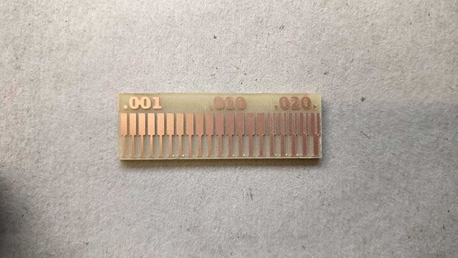
Milled Board

Changing the tool diameter from 0.4 to 0.1 resulted in trace becoming thin, but we were unable to get the desired result using default settings in fabmodules.org. We were unable to figure out what the mistake was.
Testing with tool diameter 0.1mm

From the above test it's understood that the minimum width the bit can clear is 0.016"(0.4mm) which is the diameter of the bit. The minimum trace is inconclusive as we had some difficulties in generating the right .rml file from FabModules.