i’ve created new post because i needed another clean page to include the final pcb of this this week
please check the design work flow page
Schematic Design:
this is the schematic design:
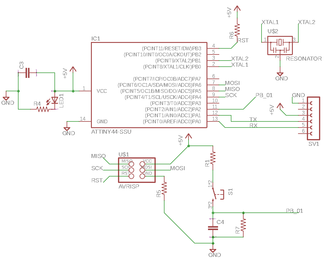
Component Selection:
- MCU attiny44
Resistors:
R1this resistor will control the charging speed of the
capacitorC4-> 10K OhmR4this resistor will limit current to prevent LED rush current:
minimum 330 Ohm5v - 1v(accros led) / 330 ohm < 12 mA
R50ohm just jumperR6pullup resistor, this drive the reset high to prevent mcu from reseting
and limit the current when the programmer short it to ground…R7to control the discharge ofC4when the button unreleased this resistor
provide path to discharge capacitor, 10k OhmC4this capacitor will charge and discharge when the button (pressed/released)
100nF
Pcb design:
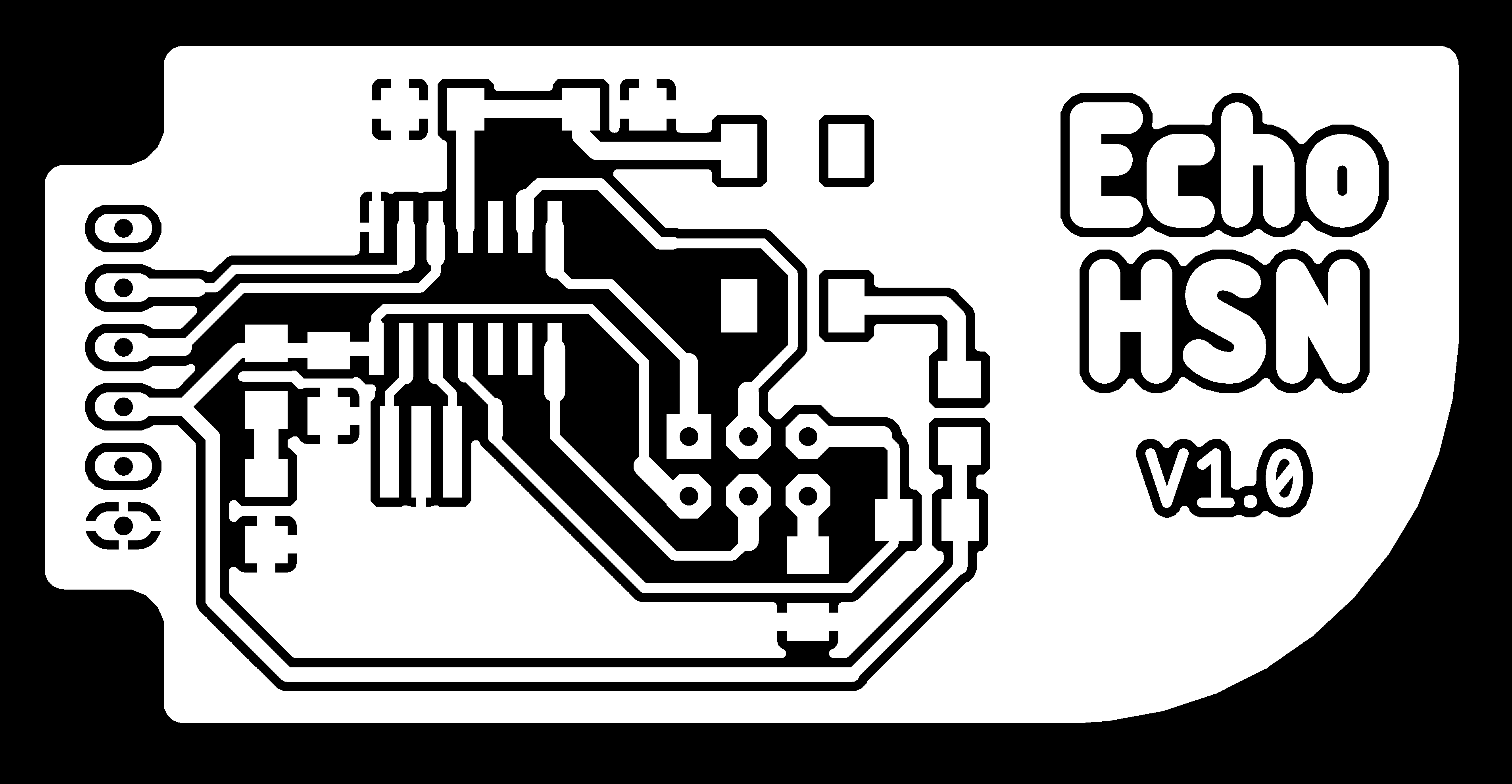
this is the final pcb .. for technical details you can view the
Design Considerations and tips
#design-considerations-and-tips
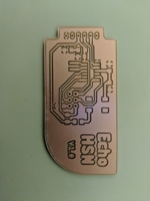
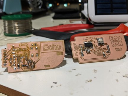
v1 tx - rx
v1 programming
in this post i’ll talk about my experiment in designing the electronics circuit “Echo”
First, the goal of this assignment is to try circuit design from schematic, pcb, and produce the physical circuit
the circuit was orginally designed by Neil:
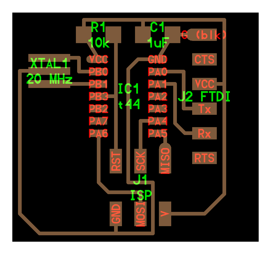
to start with i’ve downloaded Fab library for eagle which contains the available components
the library is installed in eagle/lbr folder
then the schematic is straight forward, its attiny45 microcontroller that is connected to icsp programming pins and to FTDI chip to communicate through usb
i used eagle in order to draw the schematic and the pcb
Schematic Design:
for the schematic circuit design:
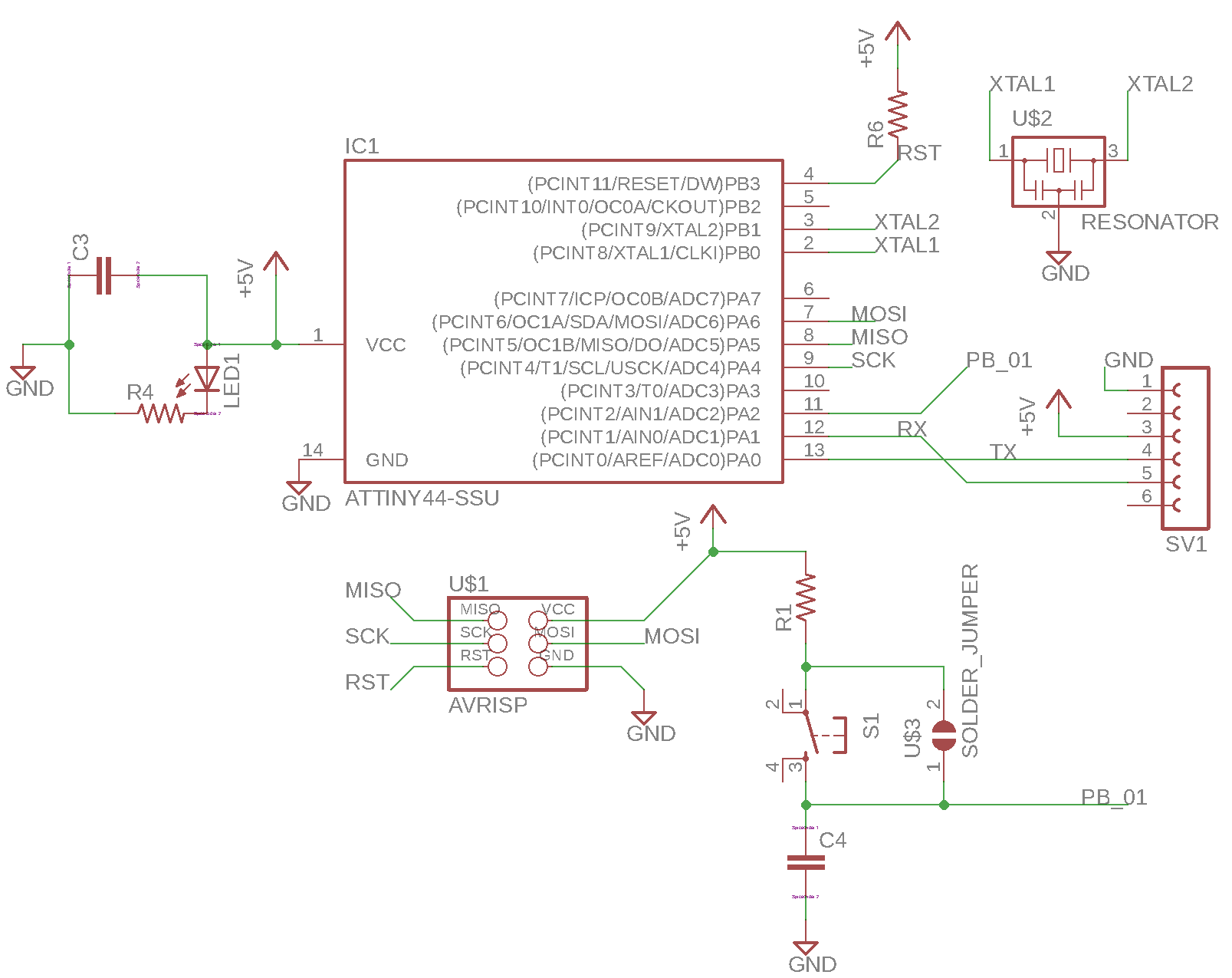
as can be seen in the picture the following components are used:
- MCU attiny45
- LED -> connected to power to detect the circuit is working
- AVRISP header -> through hole package
- 20 MHz crystal with internal capacitors
- FTDI headers -> through hole 6 pins female
- PushButton circuit:
the push button is connected to a capacitor which prevents the change in voltage and slow down the signal this is because i want to elimenate the bouncing of the push button
problem 1:
the sch file is connected directly to the board file in eagle software and when i changed some compnent
i got the following error:
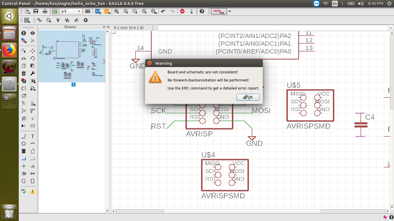
Pcb design:
for me, most important thing in this design is to place the crystal oscillator and decoupling cap near the mcu
so i started placing the components and routing
unfortunately didnt take picture of the initial circuit design,
i used 3 of 0 Ohm resistors as jumpers because i used small pcb layout …
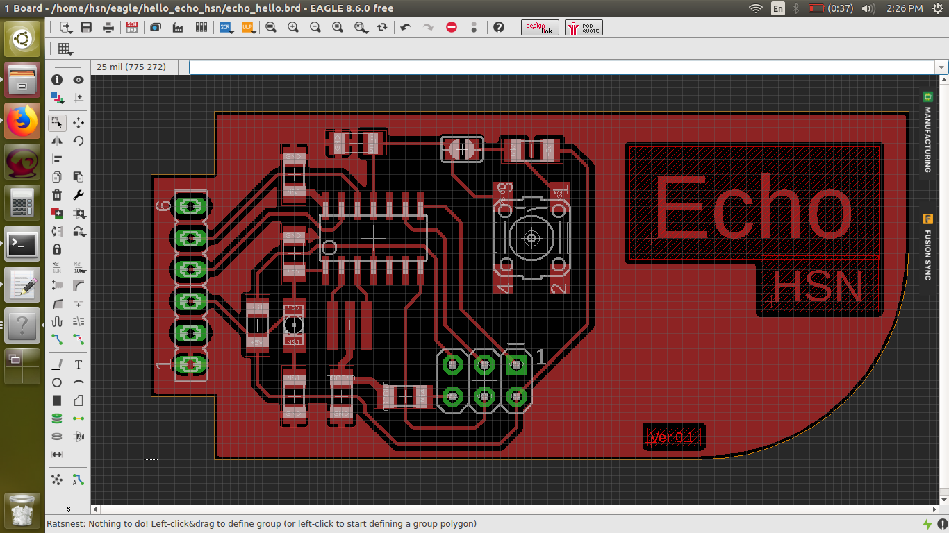 in order to mill the circuit, i ve to export it to PNG file for the fab module..
But Wait …
inorder to export the png file .. i’ve to export the milling part for the 1⁄64” drill bit here are the steps:
click on the layer tool
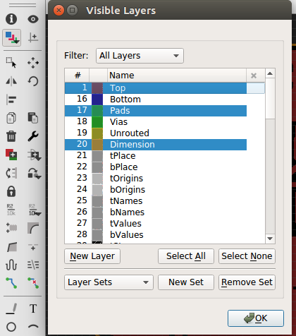 select the wanted layers to show ..
then File -> Export -> Image -> [1000] DPI & [x] Monochrome
dont forget to check design consideration tips
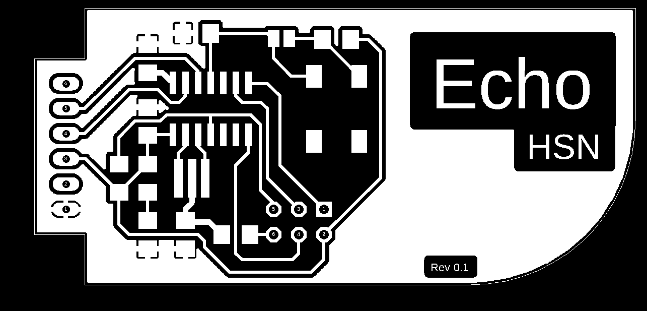
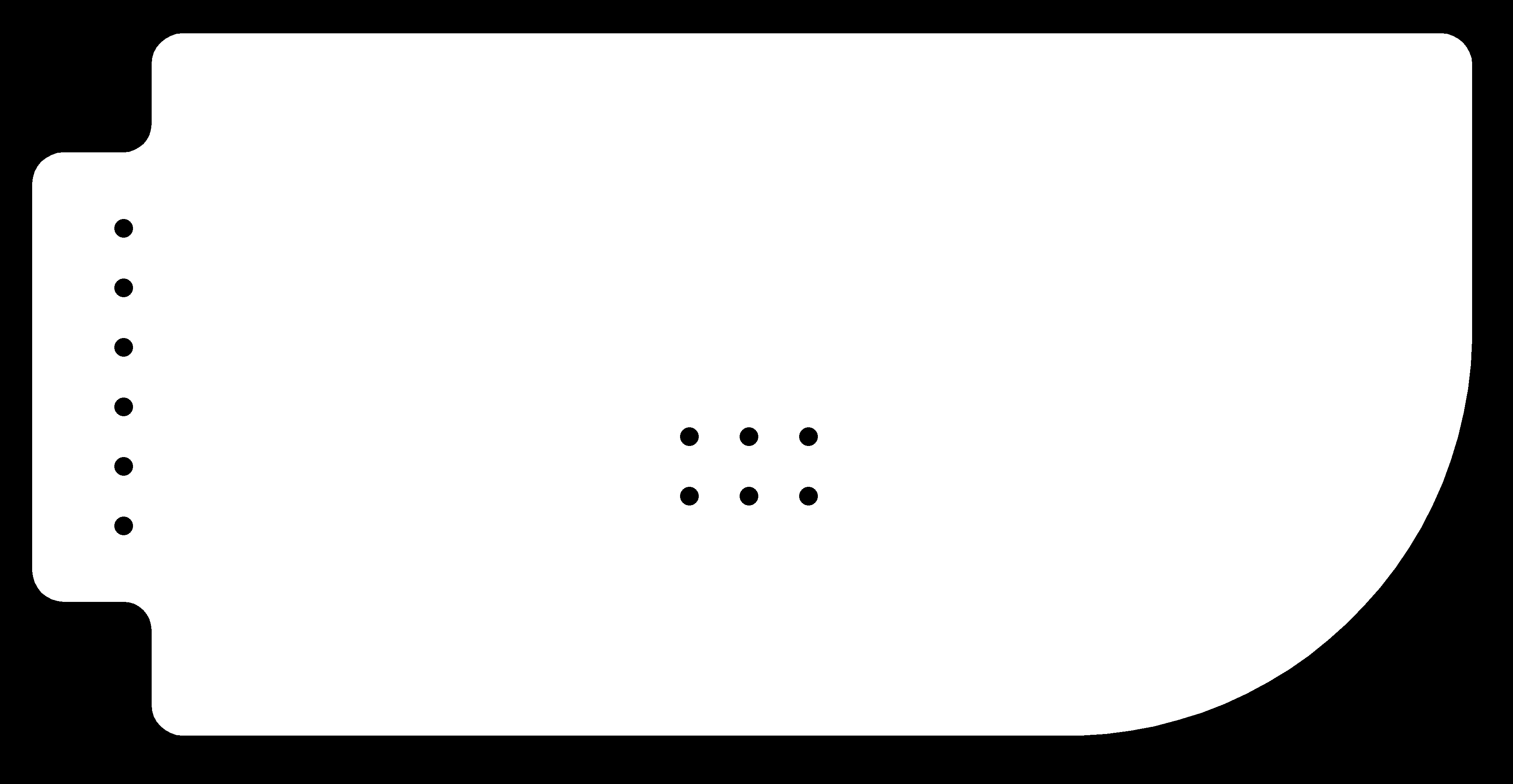
for cutting the board and drill the holes … we use 1⁄32” drill bit ..
to export that image i remove the top layer .. and export the dimensions and pad layers
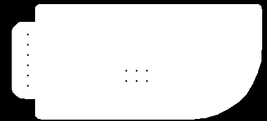
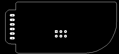 and then i fill the black area with white in Gimp editor ..
Design Considerations and tips
set pad names:
as can be shown below, when i export the pcb as png ..
it shows the pad numbers that have holes…
 this can be problem as it could be detected as path and milled ..
in order to solve that Gimp can be used to edit the image and fill the hole
however, by researching in eagle there is setting to hide them ..
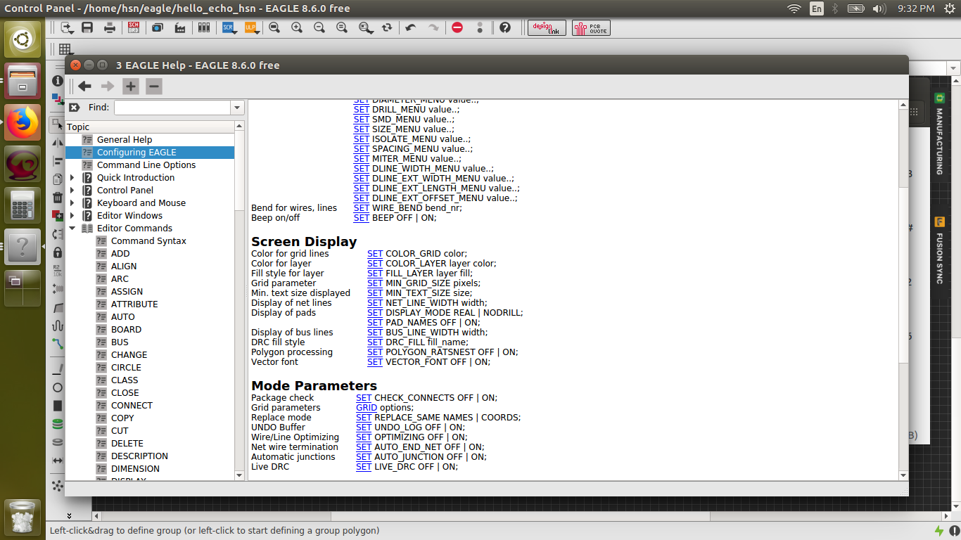
this code solves the problem :
Set Pad_names off;
navigation through ctrl:
this is good for laptop mouse-pads or mouses without middle button:
set Interface.UseCtrlForPanning 1 Panning is done by moving the mouse while holding the center mouse button (or mouse wheel) down. In older versions this was done by pressing the Ctrl key instead. If you want the old functionality back, you can set this parameter to ‘1’. Note, though, that the Ctrl key is now used for special functions in some commands, so when using these special functions (like selecting an object at its origin in MOVE) with this parameter enabled you may inadvertently pan your draw window.
DRC
for the (1⁄64” = 15.6mil) drill bit:
so i use the following parameters:
- 16 mil clearance
- 15 mil min width for track widths
- thermal pads 15 mil
- isolate for polygon:
well, when you rastnest the polygon will pour the empty area, you can right click and
select isolation for the polygon so it leaves some clearance with tracks and pads …
use ground plane
its a good practice to use ground plane…
there are many reasons for that i’ll not talk about it here but you can read for more details:
Wiki Ground plane
The EMI benefits of ground plane
PCB Design Guidelines
Manifacturing:
- drill bit problem: there was a problem, the bit was broken and the MDX-15 head had vibration, this means that when it mill the tracks it will vibrate on the small track width and make unclean cuts .. i didnt take picture of the old PCB, however, i re-milled the PCB again
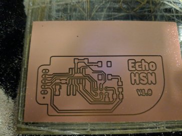
the pcb was opened in fab modules in milled in the milling machine we have…
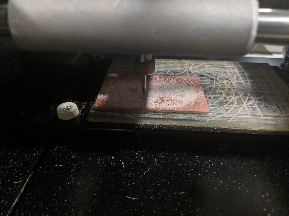
after the milling was done .. cleaning the pcb …
break the pcb from the copper plate ..
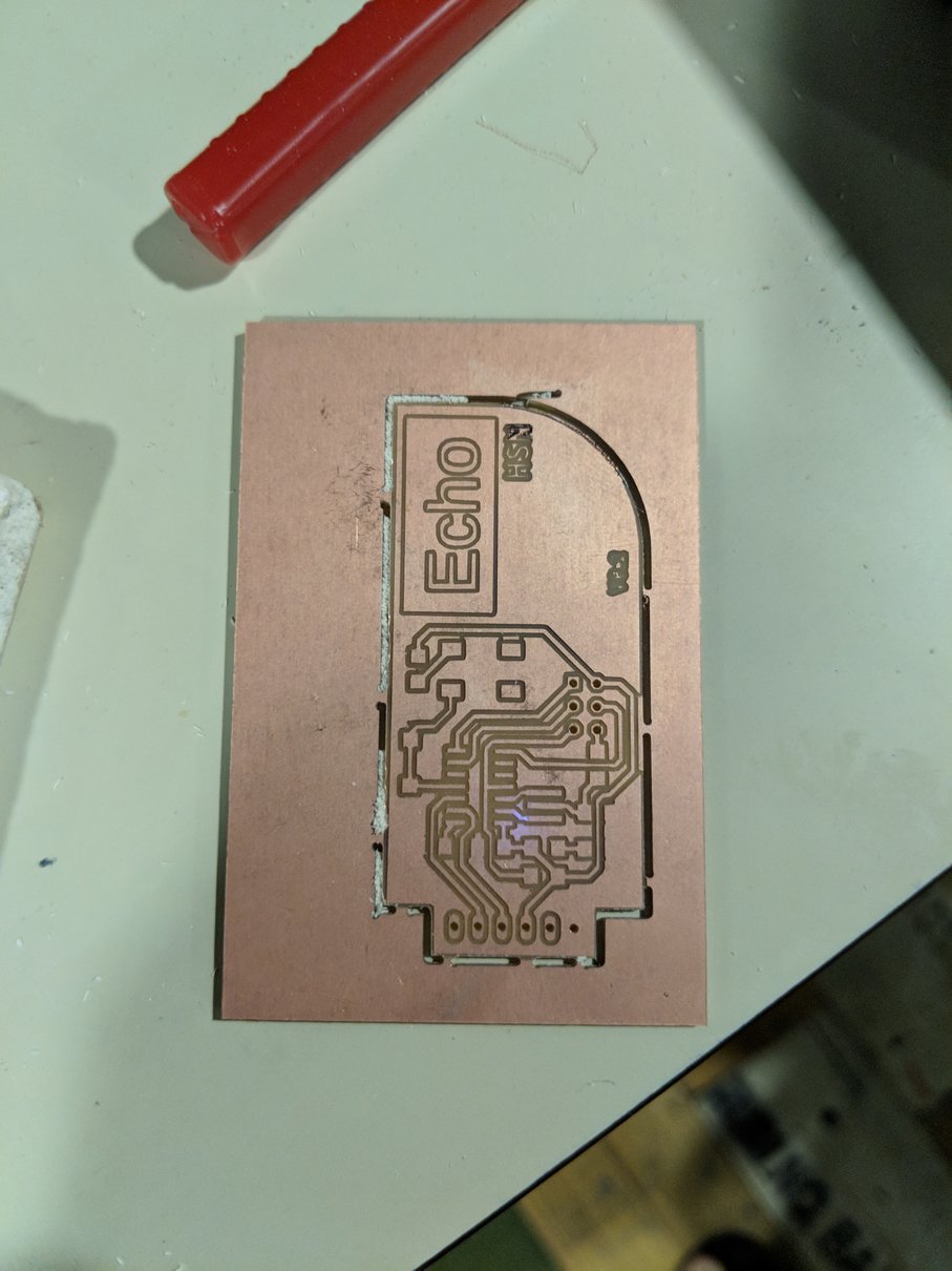
some flux before soldering :P
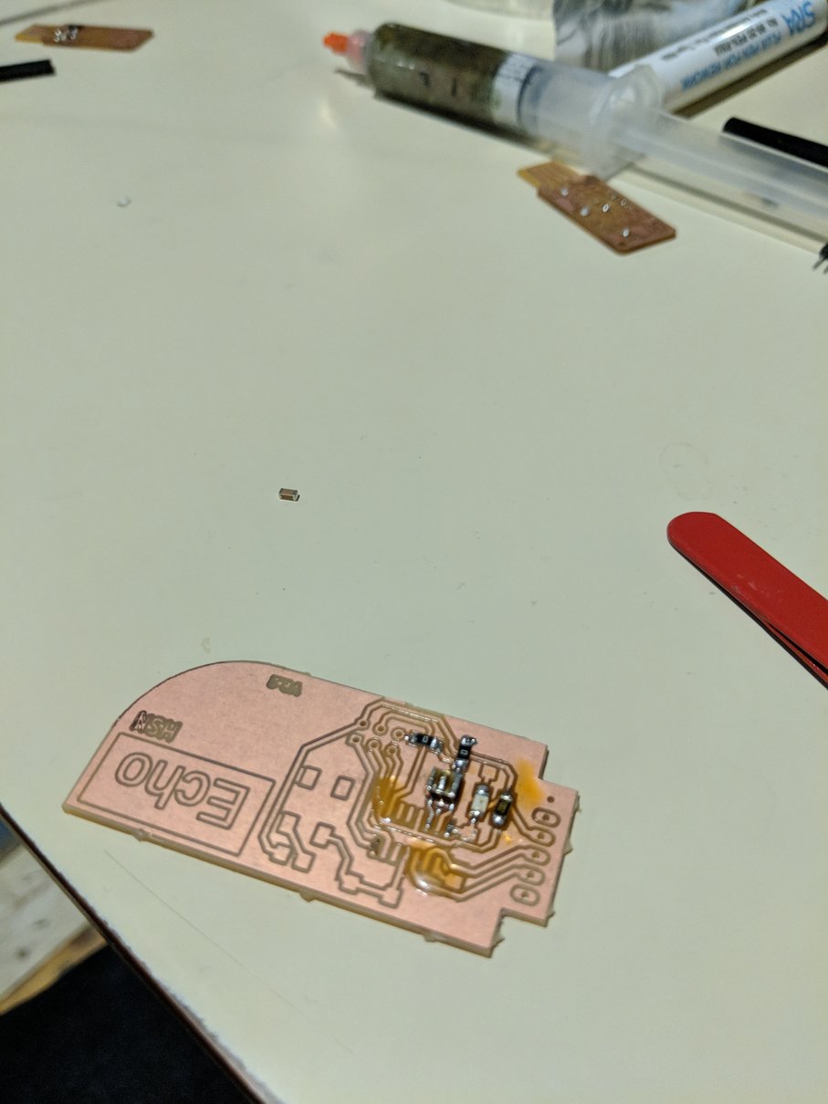
soldering the pcb ..
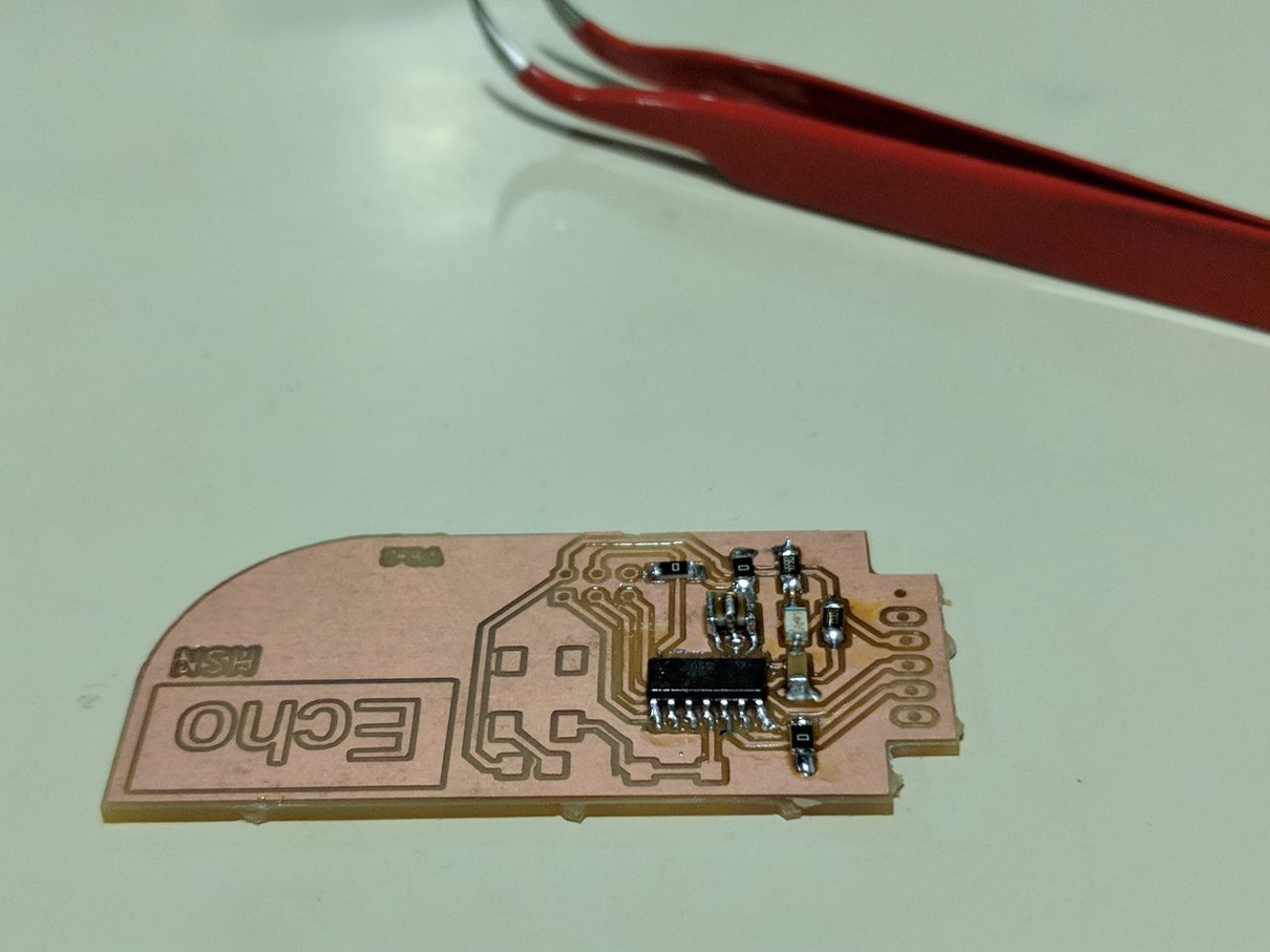
issues in connecting the avrisp ..
well, this happened because when i put a part that supposed to be on bottom plane i’ve to mirror it
so the pins where flipped ..
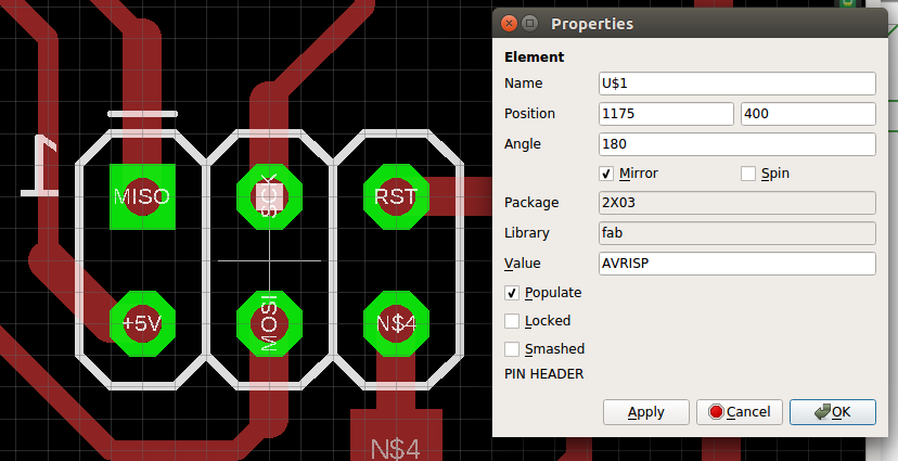
so to fix that:
after that i’ve manually connected the avrisp pins to the board:
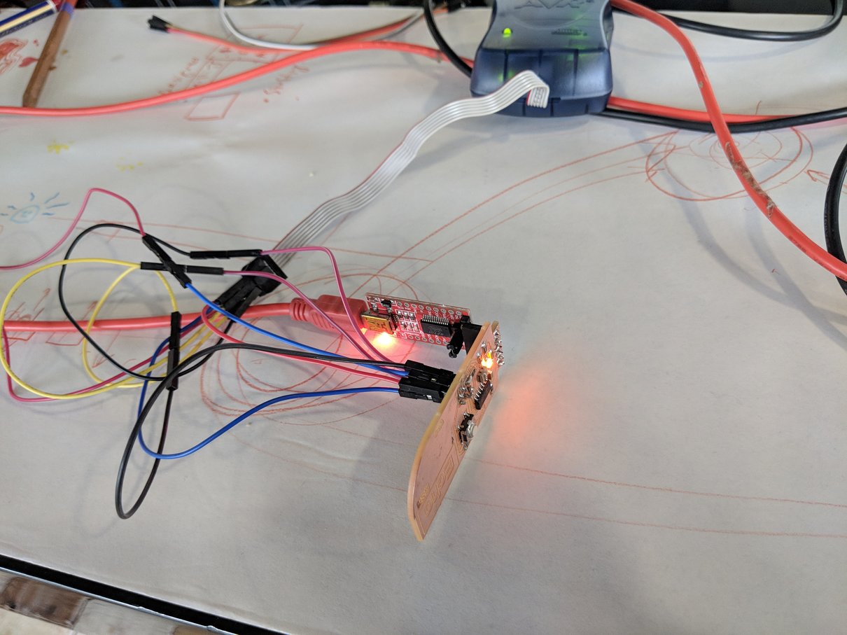
programming:
follow neil steps from HEREexcept that i used avrisp2 instead of usbtiny ..
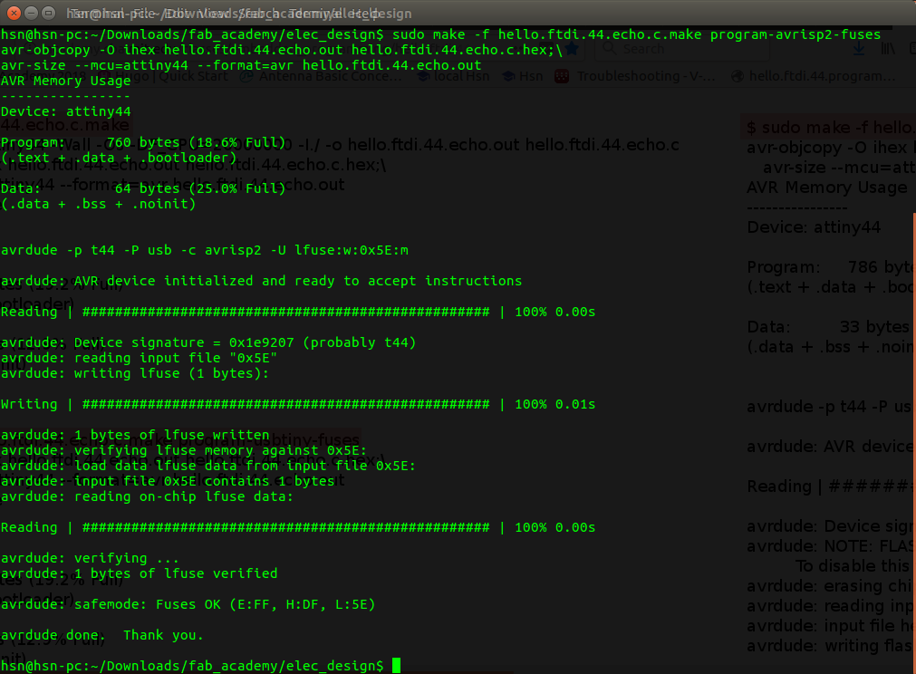
and testing:
as you can see… there is problem in aligning the string in putty this have been invistigated in week 8 .. embeded programming ..