Electronics design
This week's assignment is to design an electronic circuit, by redrawing the hello world board and adding a button and LED. And to Use the test equipment in the lab to observe the operation of a microcontroller circuit board
To create the schematic design I started experimenting with several design softwares (probably more than I should have) to find one I liked and wanted to work on. I've used Altium designer before and do own a license for it so it was one of my options. I spent waaay more time than I should have doing this assignment
- Eagle
- Circuit Maker
- Altium designer
- Eagle (AGAIN)
- Design rules
- Making
- Testing
- Group project: test equipment
- Circuit Files Download links
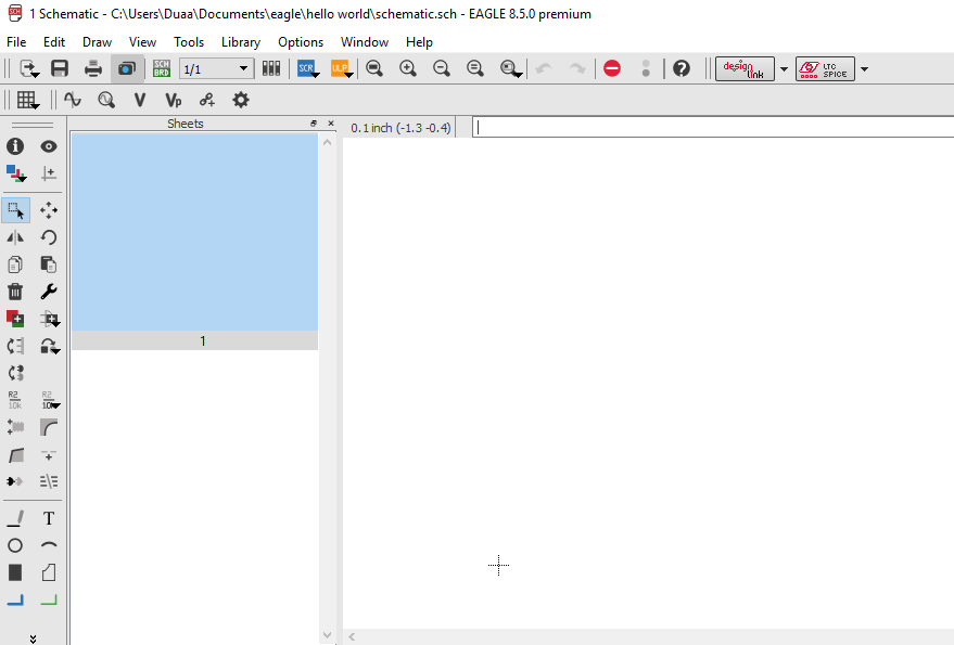
Eagle
Autodesk EAGLE is powerful, easy-to-use PCB design and schematic software.
I havent used Eagle before so I first started experimenting with using Eagle to create the schematic and the pcb as it was a software I wanted to explore and it seemed to be what everyone was going to be using.
At first I just started getting used to the settings and the environment. To create a pcb, you must create a project with a schematic file and a pcb file within it.
The enviornment in eagle took a lot of getting used to, it was kind of tricky to figure out how to do anything there since i am used to using altium designer and it has very different shortcuts to get things done. Having to select the action i wanted from the tools menu everytimer instead of right clicking on the object was very frustrating, and so was having to click right in the middle of an object to select it rather than being able to click on any part of it.
Adding the fab library in eagle was fairly easy, however I couldnt find the Fab library file, all i found was the raw code in an old github so I copied it in a text file and saved it as an eagle library which worked fairly well.
Being used to using Altium designer, I did not enjoy the use of eagle that much when trying out placing some parts and connecting them so i decided to give circuit maker which is the free version of Altium designer a try.
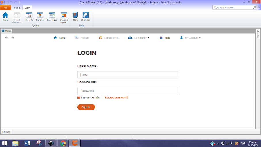
Circuit maker

CircuitMaker is electronic design automation software for printed circuit board designs targeted at the hobby, hacker, and maker community. CircuitMaker is available as freeware, and the hardware designed with it may be used for commercial and non-commercial purposes without limitations.
Circuitmaker is a community based program, so you must create an account (free) and you have to be logged in and online to use it.
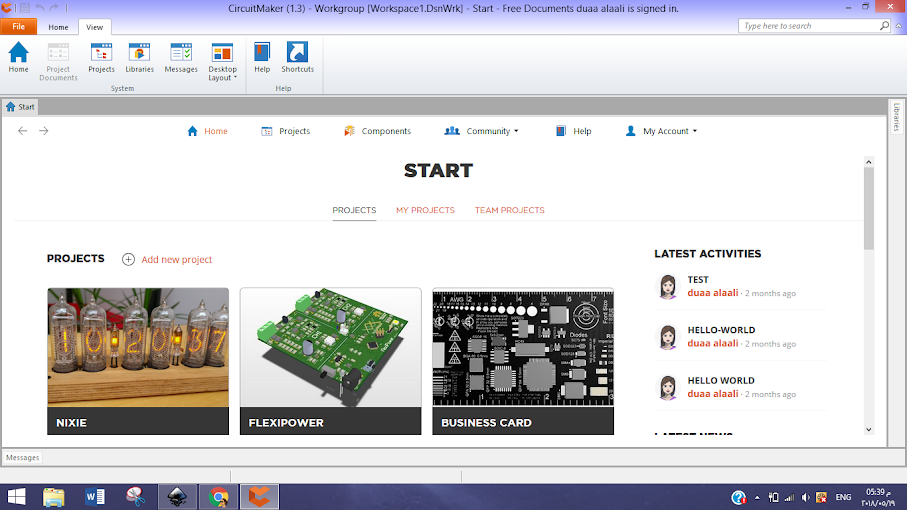
I created an account and started exploring.
I really liked the community aspect of circuitmaker, you can see projects that other people have made and share your own, you can also collaberate with others on a mutual project by forming a team. I think all of that is really great and could possibliy be used in the future to collaberate on shared projects using the circuit makerplatform.
However, I couldnt find the fab library to add in circuit maker so i can get started with my circuit, and after quick google search I found out that you can add parta individually ( i could be wrong) and there isnt a direct way to add a library.
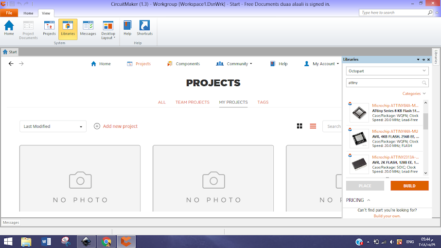
clearly, trying to find all the parts i need by looking them upin the circuit maker component online search platform was going to be time intensive since i need some very spicific part, i decided to not use circuitmaker for this assignment. This does not mean i dislike it, I am planning to start exploring it for other uses.
Altium designer

Altium Designer is a PCB and electronic design automation software package for printed circuit boards. It is developed by Australian software company Altium Limited.
Altium designer is not a free software, I owned a licesne. It is one of the best and industry leading PCB design tools. I personally love Altium designer becuase I am used to it and have used it a lot before.
The first step I did was add the Fab library in altium so I can get started and design my circuit.
To add a library in Altium designer, first you must right click and select place part
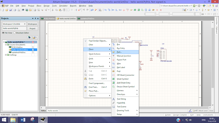
Then navigate to libraries and pick the location of your libray file.
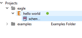
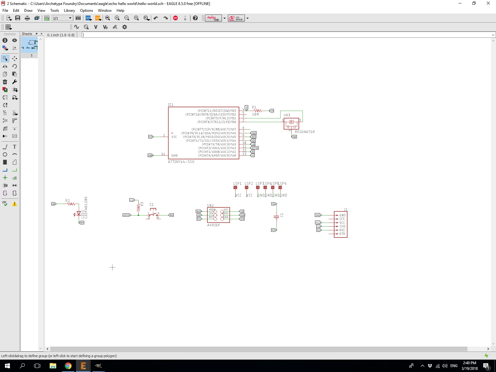
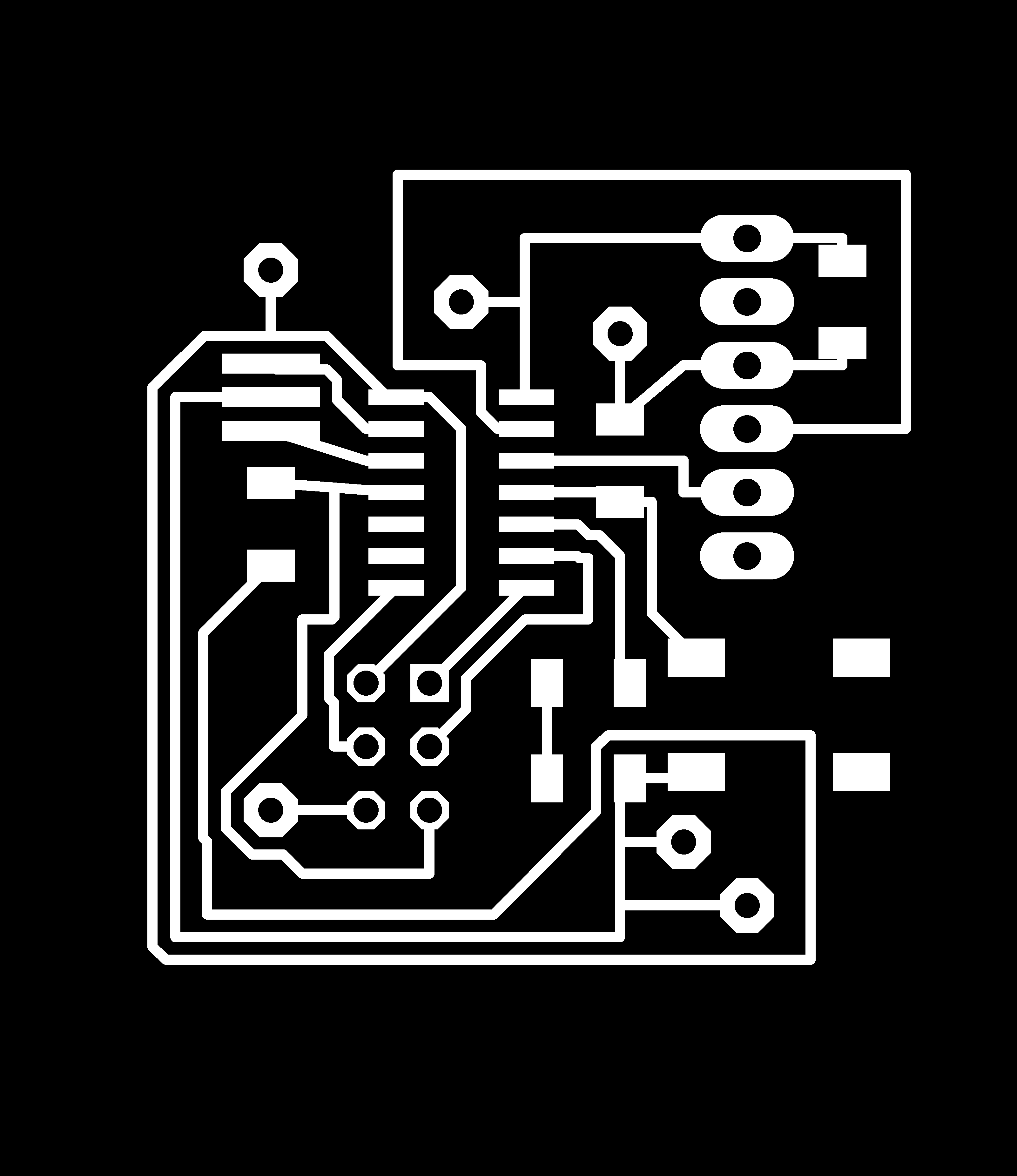
After adding the fab library it was now time to create the schematic of the circuit and the PCB. I am recreating Niel's hello world board and adding to it one button and one LED.
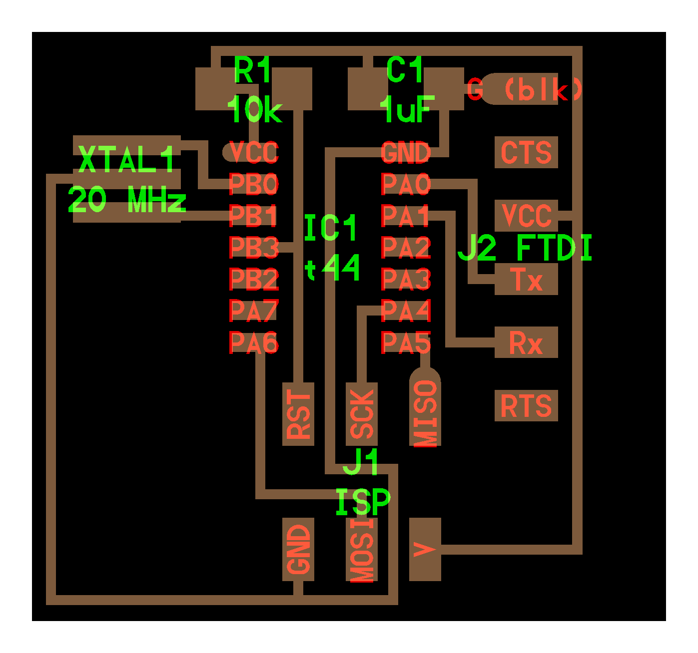
Creating the schematic in Altium was fairly simple. I added all the parts that I needed from the Fab library using the place part command. I connected everything together in the schematic.
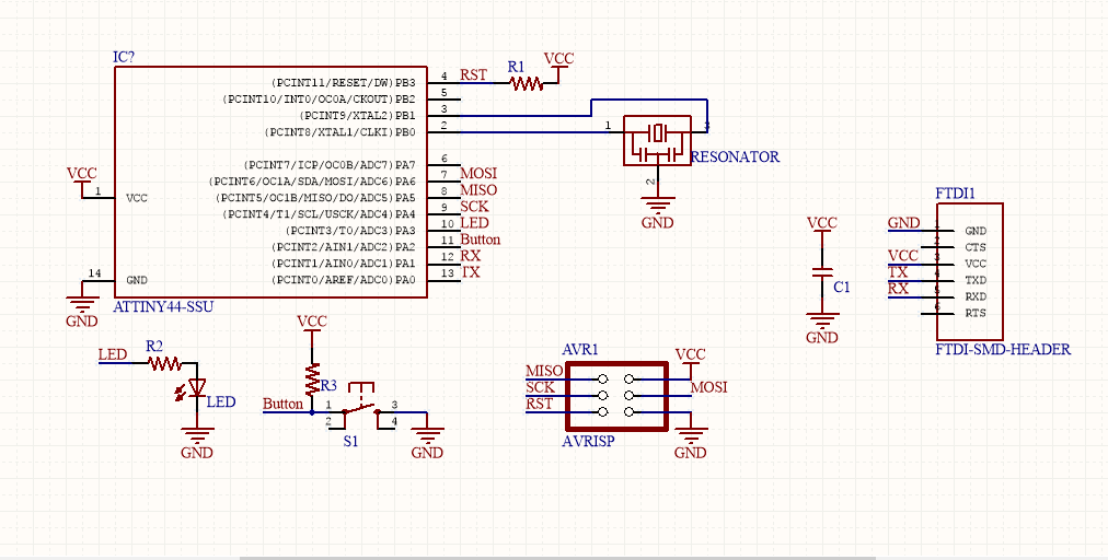
I have an ISP and FTDI header. The compoonents are connected using net labels, and with that it is time to create a PCB.
The easiest way to create a pcb in Altium is through the pcb board wizard which allows you to select your board options.
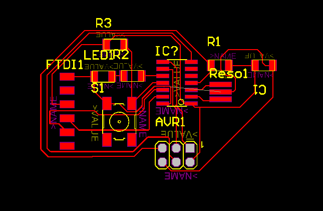
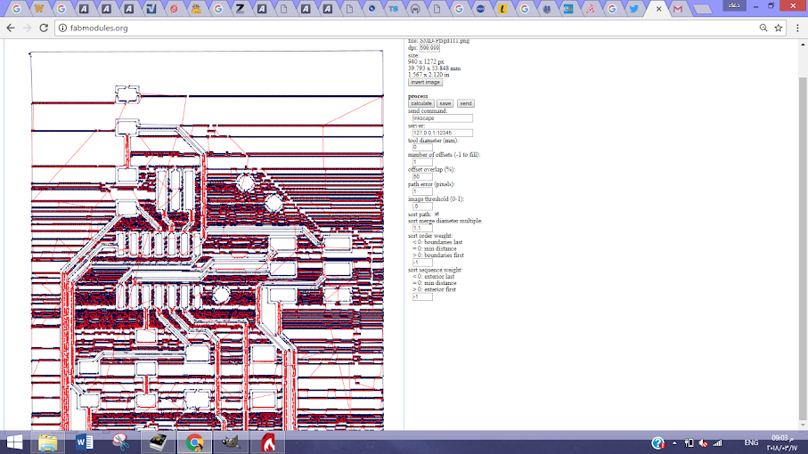
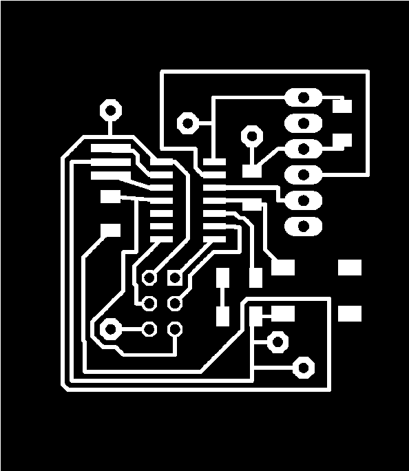
Next was the tricky part, getting the pcb in image format to be able to mill it through fab modules. It is not straight forward like in eagle but it is possible. I followed the steps from this helpful guide.
What was different about my PCB however, was that I was using some through hole components. I could not find a way to export my through holes in a seperate image. Another issue was that i was using a polygon pore and connecting that to ground, it gave me avery weird output when converting it.
Besing short on time, I couldnt figure out a way to fix my issues exporting the pcb from Altium and I just had to quickly recreate it in eagle to be able to complete my assignment on time.
Eagle - take 2
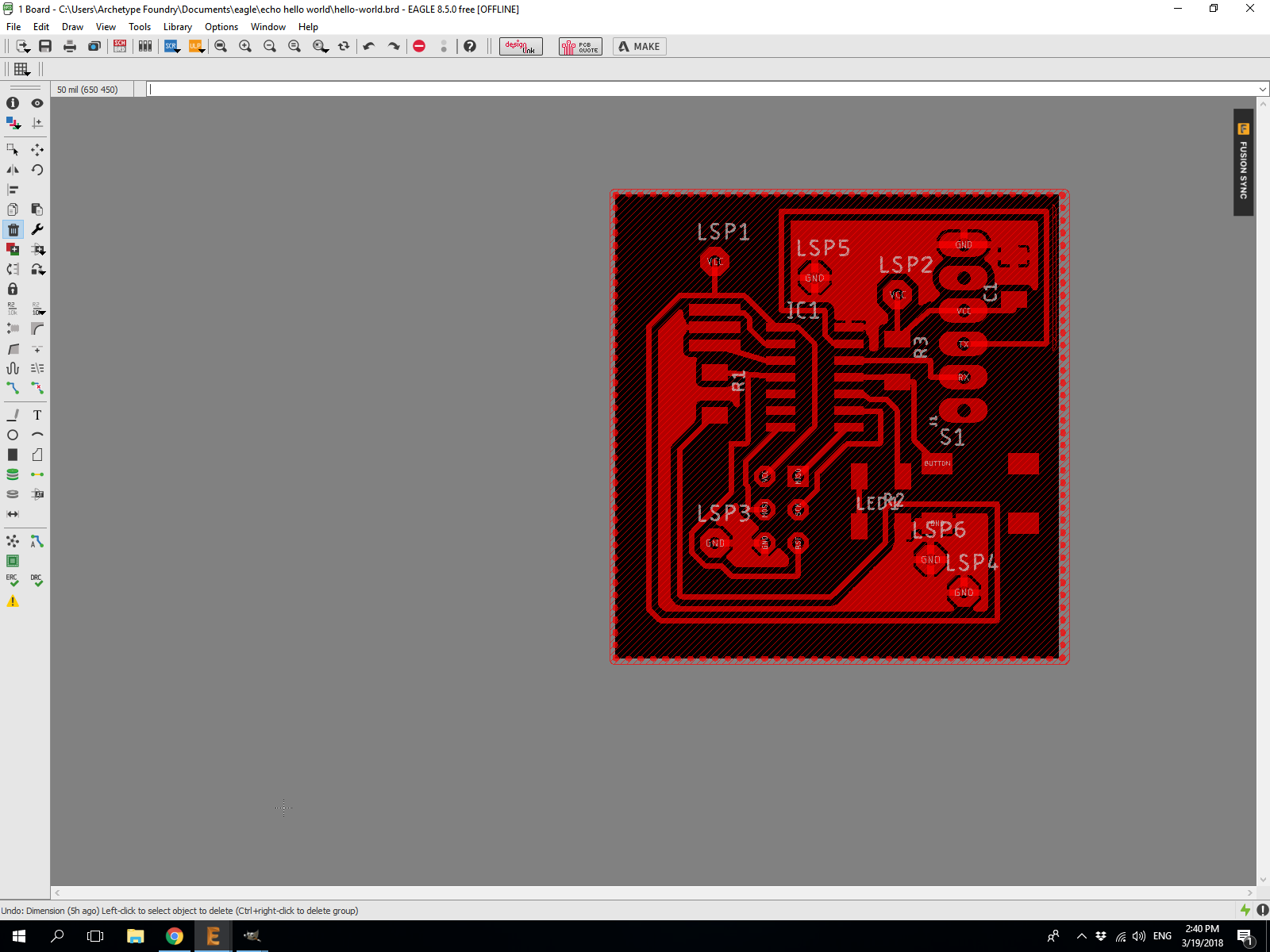
eagle's shortcuts took so long to get used to. the fact that i already made the schematic and PCb helped a lot in speeding up the eagle recreating process. Eagle is a pretty great program once you get the hang of it. It has a lof of the tools Altium has and it did not take me that long to recreate the schematic and PCB. it did however requie a lof of googling and watching tutorials to figure out how to do a lot of the functions like update the PCb when updating the schematic.
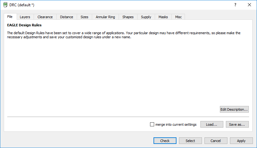
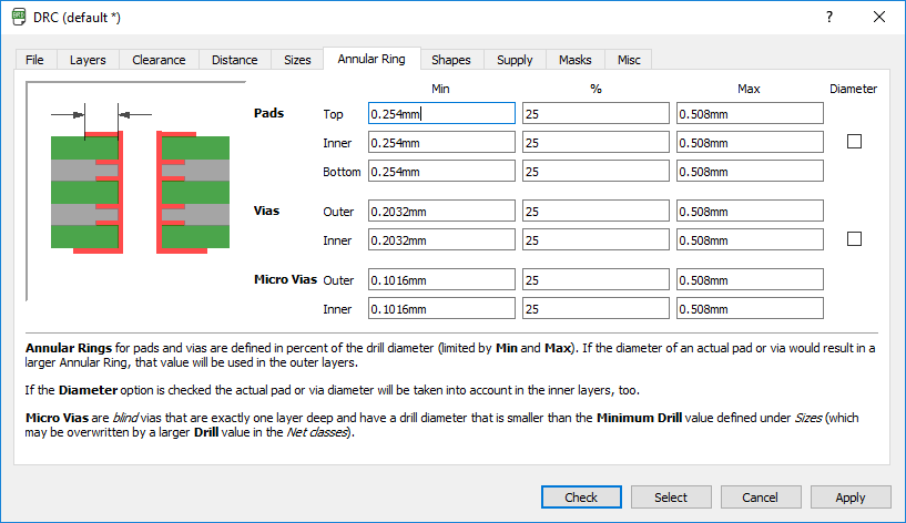
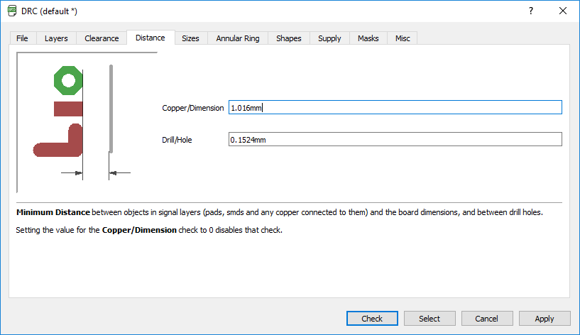
Design rules
Before milling the circuit it is a good idea to check the design rules of the pcb to insure it will print right. Important factors include track width as the mahine wont be able to mill it right if the tracks were twqo small, also the clearance between tracks and components. this is important becuase the machinbe wont be able to mill it right depending on the milling bit size, the accuracy of fab modules and even if it did, an over crowded pcb is hards to solder and it is very easy to get small solder bridges that will mess the board up.
To get to design rules select Tools > DRC
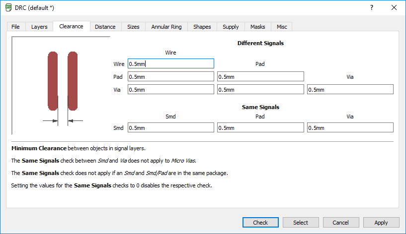
I am using 0.5 mm clearance between everything on the board
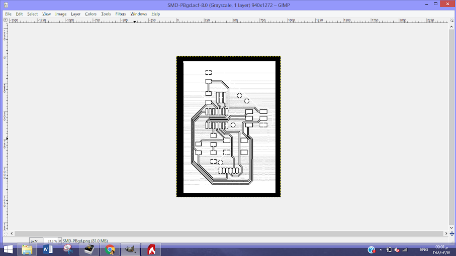
Exporting a PNg for fabmodules on eagle is extremely easy. All you have to do is select the layers you want appearing in the image. I am doing it twice because I am using throughhole components so it is a little different than using SMD only components.

Making the board
I milled the board on a roland MDX-15 using fab modules. I used 1/64 inch bit for the inner tracks and 1/32 for the boarder and for the through holes.
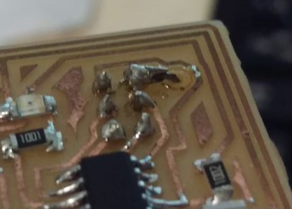
I made jumpers using throughhole components as I could not directly connect my tracks in some cases. I would not reccoment doing that. using 0 ohm resistors is much easier.
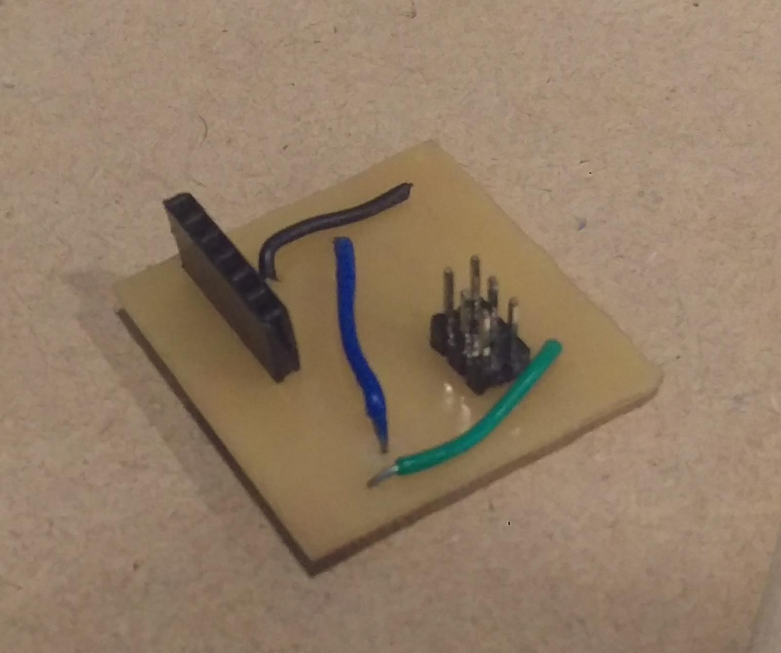

using through holes is a bad idea becuase they get drilled in the middle of the pad, which makes the pad weak and easy to rip out, which actually happened to me. I tried to force one of the jumpers in with a pliar after partly soldering it and the whole pad ripped out.
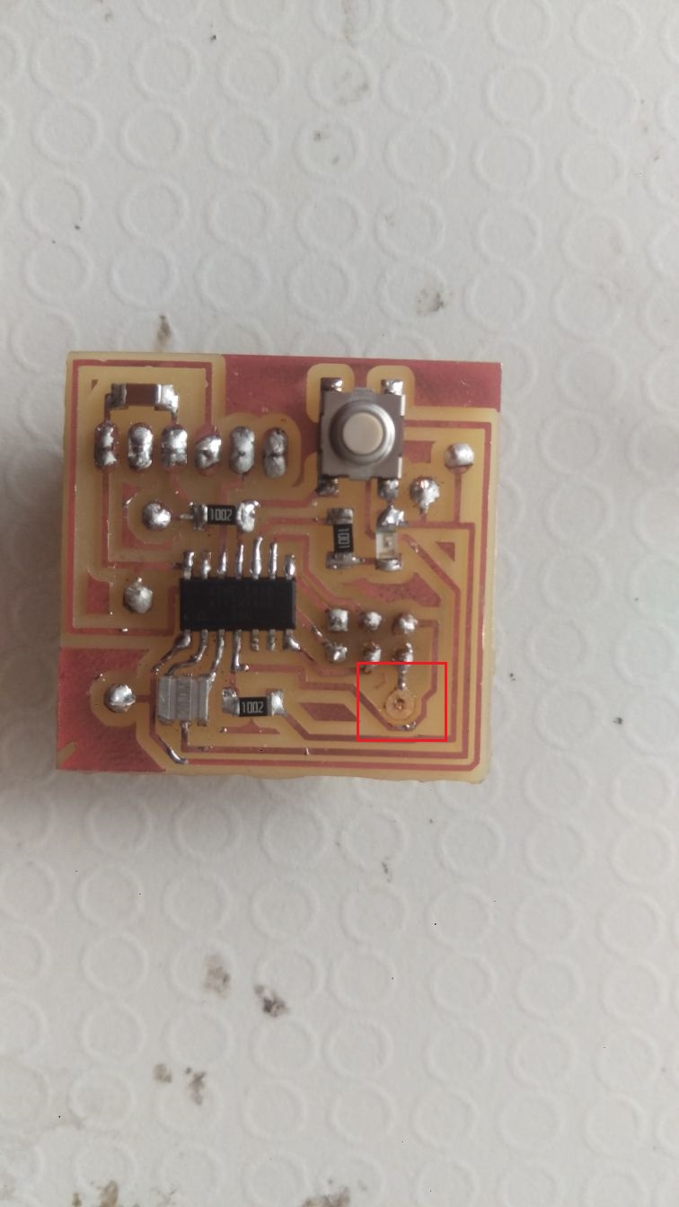
I had to improvise and connect the jumper to the next pad instead.
Testing the board
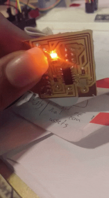
For testing the board I connected it to my programmer and started programming it through the arduino IDE. I just did a simple button controlled LED test to check its operation.
 const int buttonPin = PA2;     // the number of the pushbutton pin
const int ledPin =  PA3;      // the number of the LED pin

// variables will change:
int buttonState = 0;         // variable for reading the pushbutton status

void setup() {
  // initialize the LED pin as an output:
  pinMode(ledPin, OUTPUT);
  // initialize the pushbutton pin as an input:
  pinMode(buttonPin, INPUT);
}

void loop() {
  // read the state of the pushbutton value:
  buttonState = digitalRead(buttonPin);

  // check if the pushbutton is pressed. If it is, the buttonState is HIGH:
  if (buttonState == HIGH) {
    // turn LED on:
    digitalWrite(ledPin, HIGH);
  } else {
    // turn LED off:
    digitalWrite(ledPin, LOW);
  }
}
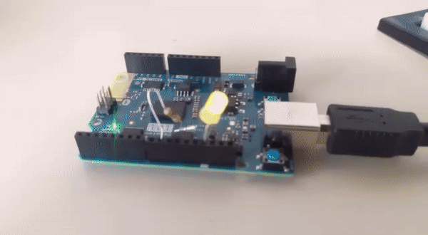
it worked ( i was very surprised i managed to get it working immediatly without any soldering retouching). I was able to control the LEd using the button.
test equipment
the purpose of this assignment is to Use the test equipment in the lab to observe the operation of a microcontroller circuit board.
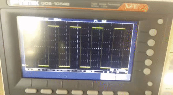
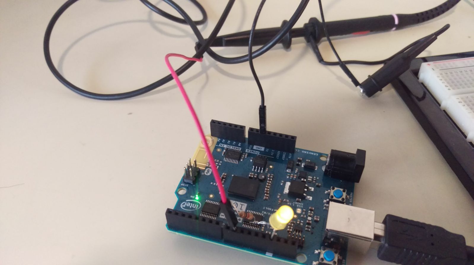
I am using one of the most famous microcontroller circuit boards, an Arduino. i am using an arduino 101. I used an oscilloscope which allows observation of varianing signal voltages.
I was observing how exactly two of the most famous arduino codes happen exactly. A blink code and a fade code.
Starting with the blick code. I am using an LED connected to pin 12 of the micrcontroller and observing how it gets toggled on and off by the microcontroller.
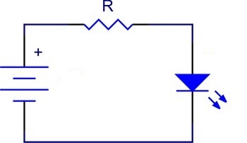
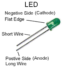
First to connect the LEd I am using a 1K pullup resistor to avoid damaging the components. you can know what side is the cathode and anode cause one of them is longer than the other. LEDs must be connected at the correct polarity
// the setup function runs once when you press reset or power the board
void setup() {
  // initialize digital pin 12 as an output.
  pinMode(12, OUTPUT);
}

// the loop function runs over and over again forever
void loop() {
  digitalWrite(12, HIGH);   // turn the LED on (HIGH is the voltage level)
  delay(200);              // wait for a second
  digitalWrite(12, LOW);    // turn the LED off by making the voltage LOW
  delay(200);              // wait for a second
}
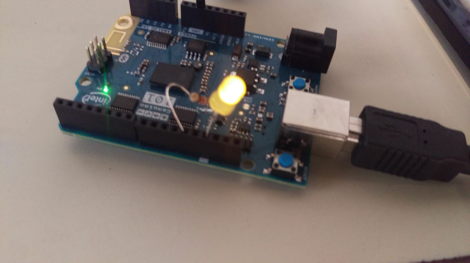
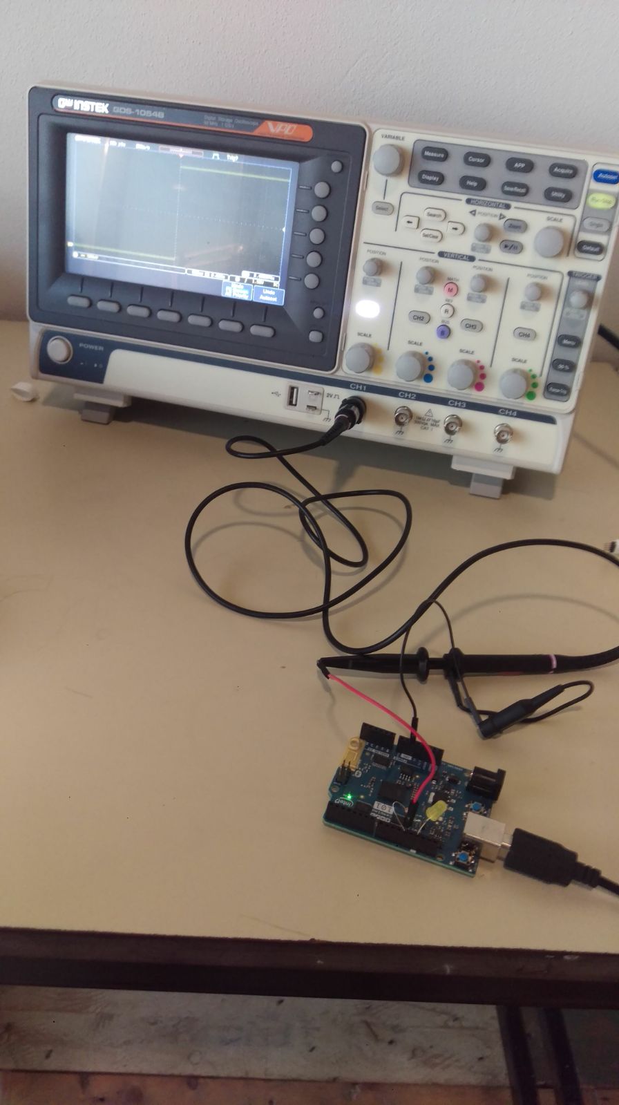
as observed via the osciliscope, the output from pin 12 is turning on and off really quick at 5v and 0V thus the LEd turns on and off really quick along with it.
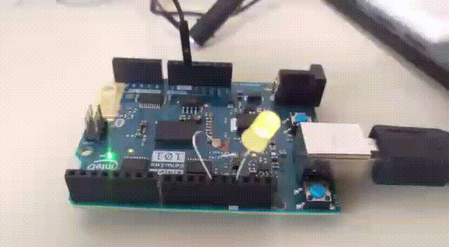
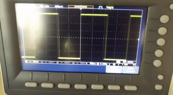
Lets move on to observing the fade code.
 int led = 9;           // the PWM pin the LED is attached to
int brightness = 0;    // how bright the LED is
int fadeAmount = 5;    // how many points to fade the LED by

// the setup routine runs once when you press reset:
void setup() {
  // declare pin 9 to be an output:
  pinMode(led, OUTPUT);
}

// the loop routine runs over and over again forever:
void loop() {
  // set the brightness of pin 9:
  analogWrite(led, brightness);

  // change the brightness for next time through the loop:
  brightness = brightness + fadeAmount;

  // reverse the direction of the fading at the ends of the fade:
  if (brightness == 0 || brightness == 255) {
    fadeAmount = -fadeAmount ;
  }
  // wait for 30 milliseconds to see the dimming effect
  delay(30);
}
You will notice from the code that i moved the LEd to pin 9. That is becuase the fade is controlled by PWM and pin 9 has PWM capabilities. It works by changing the pulse width modulation up and down really fast to make the led brigtness change.
Circuit Files Download links
Eagle schematic file download linkEagle PCB file download link
PNG tracks PCB file download link
PNG throughhole PCB file download link