The process!
First thing's first - download Eagle! As per the recommendation, I downloaded the free version of Eagle from AutoDesk.
I also downloaded the parts library from http://archive.fabacademy.org/archives/2017/doc/electronics/fab.lbr to use in Eagle.
I also need the actual board itself that I'm making, since I have no idea what it is, so I used the helpfully provided link to the echo hello world board:
http://academy.cba.mit.edu/classes/embedded_programming/index.html#echo
And will be making the one called hello.ftdi.44.
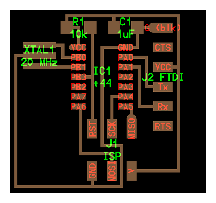
So it looks actually simple enough. And looks like we'll be using the ATTINY44 microprocessor.
The actual list of parts, from the looks of it, appears to be this:
XTAL 20MHz resonator
10k ohm resistor
1u farad capacitor
ATTINY44 microprocessor
A 6 pin connector for programming (just like the one used in the programming board making)
Another 6 pin connector but a flat one this time
These are deceptively few components, but we should also add at least one button and one led diode to it, in addition to the list of components above.
I've never actually used Eagle before, and since I missed the last days at the lab for virulent reasons, this will be my first time even seeing one.
I'm going to follow several of past year's documentations to try and get an idea on how to best use the software to make the design, and intend for this documentation to be a representation of my going from 0 knowledge of Eagle to 100% of the necessary knowledge to design this board :P
So first I click on File > New > Schematic, which should obviously create a new schematic for me to work with.
.jpg)
Okay, now what?
I think, I need to add some components, so let's click "Library".
.jpg)
Okay, and now let's Open Library.
.jpg)
Aha. Okay, this is the fablab library I downloaded, so I'm gonna open that. And now I got this screen:
.jpg)
With a whole bunch of components. So I'll add the components that I need from that.
.jpg)
Okay, so this is like, what, a schematic within a schematic? Let me try to sort this out…
some time later
Aha, okay I get it. I need to click "Add" on the lefthand menu:
.jpg)
.jpg)
There:
.jpg)
But now this ATTINY44 is dragging around my cursor despite the fact I already placed one. I suppose I click the "Stop" button at the overhead menu bar:
.jpg)
Yes, that's correct. No more floating chips.
Okay time to add the rest of the components! I'm gonna follow the list I made above.
First the XTAL resonator:
.jpg)
Boy, I'm spoiled for choice here. There's so many :/
None of these options actually appear to be the correct choice, based on the schematic received from Emma:
I have a feeling that XTAL simply stands for "Crystal", and not a particular model. So let's try again but this time search for "Resonator" instead of "XTAL":
.jpg)
Aha, looks correct now. Looks like the right resonator is simply the one called "RESONATOR" in the fab library I downloaded. Added it!
.jpg)
Okay so I'm not going to add a screenshot of every single component that I add, but the logic is fairly simple enough to follow.
Note from mid-process - adding the button is actually not straightforward. There's nothing named Button! Instead it's found as "6MM_SWITCH". So I added that. But I found it manually by checking every item and seeing which looks the most similar to the schematic sent by Emma our instructor.
And here it is!
.jpg)
I actually think I should also add some Grounds, VCC, another 6pin but of different appearance, and change the capacitor. So here's the actual schematic I'm at after these changes:
.jpg)
I could not find the exact 6pin connector portrayed in the schematic emailed us so I simply used a generic 6pin I found among the libraries.
So now I have all these different parts on my schematic. I presume that I can select them and change their various text details, since I obviously need to do that, so let's give it a try with the resistor.
.jpg)
Yep, that selects it. And now - Right click, and select "Attribute"?
.jpg)
.jpg)
Okay so let's try adding some attributes then.
.jpg)
.jpg)
Okay so I added an attribute but there's no actual visual representation in the schematic of what it is. So that's not it. Going back to the attributes - there's the little "Display" column showing "off":
.jpg)
So I changed that to "Value" and now there's a 10K showing up:
.jpg)
But it's not really in the right location, it should be under the resistor, not like, inside it, and hardly visible.
Okay so instead of "Attribute" I'm going to right click and select Properties!
Here I have a "Value" for the part section:
.jpg)
.jpg)
I wrote 10K there and it's now actually showing up the right way:
.jpg)
Great! So I deleted the Attribute, and am gonna go ahead and add various values to the different parts under "Properties".
Mid process note - I was having a really hard time editing certain components, like that pretty 6pin connector, and ended up "accidentally" deleting it :(
Added a new one though!
This time I actually found the correct one, called "AVRISPSMD". Catchy.
I also found the correct other 6pin, called "FTDI-SMD-HEADER", and the correct capacitor the fab library as well called "CAP-UNPOLARIZED".
So here's the new schematic:
And there's a little "Move" icon at the left hand menu, so I'm assuming I can move my components with it. Let's select the resonator, and hit the move icon:
.jpg)
.jpg)
Yep.
So at this point, I feel I should first arrange the different components together and connect them to correspond with the board image from before.
This so I can first understand the actual configuration of it, and then will have an easier time incorporating the button and led diode. So I place the image and the Eagle screen side to side:
.jpg)
And work moving the parts from there. I'll also use the "Rotate" button on the left hand menu, right under the "Move" button, to rotate the various components (if I need to). I will also work side by side with the schematics image.
.jpg)
.jpg)
Now I'd like to start connecting them, to get a better idea. So… How do we make connections in Eagle?
In the documentation website of a 2017 student from WOMA (Belgium/France), named Yassine Bruneau:
http://archive.fabacademy.org/archives/2017/woma/students/198
There's an explanation on how to get connections.
.jpg)
Click, click:
.jpg)
Yep, that's right. So all of them connected:
.jpg)
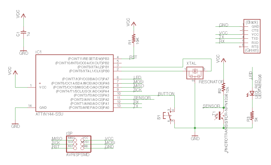
And I'm just gonna go ahead and but the button on the VCC line for a simple on/off switch, and connected the led diode to the PA7 connection on the ATTINY44 like it is in the schematic.
On second thought, I'll do the button exactly like it is on the schematic too, to control the led instead of the power.
.jpg)
Ta da!
Now of course, this is not an ideal looking schematic. But it's simply what I needed in order to understand what exactly it is that I'm making.
Now I'm just going to re-draw this schematic to be a lot more organized.
.jpg)
There, that looks much better.
Now I need to design the actual board itself.
From the same 2017 student website mentioned above, this is documented as such:
.jpg)
First I remove the first board I designed (coz it's ugly and exists as another layer, and I don't know how this might mess up my board drawing), and then I do as the 2017 documentation guides me.
I'm seeing this:
.jpg)
So… Now, I do traces? But it's all a mess here, so first I guess I'll move some parts around, do some rotations, just give it an orderly appearance. And now that I'm looking closer, I should actually connect the button at connections 2 and 4, not 1 and 3:
.jpg)
So I'm actually going to connect them correctly. when doing the PCB design itself. After moving some components around, here's what I'm feeling comfortable to start with:
.jpg)
Okay, so this actually looks kind of complicated to get all properly hooked up, but there ain't no better way to know than to try!
.jpg)
So it looks like I kind of backed myself into a corner here, with having some necessary connections that can't be actually routed, and just generally a design that's way too inefficient (in terms of material and size).
So I gave the auto router command a quick try:
.jpg)
And can kind of see what it should look like. So first I change the button connections in the schematic to be correct, and then re-ordered my components again:
.jpg)
And then I call the auto router again:
.jpg)
It kind of looks like there's some connections that need to be passing through other connections, which is no good. I have a feeling that this is because of how my board is organized, so I reordered it again:
.jpg)
And auto routed:
.jpg)
This time it looks like there's no connections passing through other connections, and it actually looks quite good. Let me see what happens if I make the route thicker, say, 10.
.jpg)
.jpg)
Well, it looks like it did not take the thickness into account when auto routing, and I also no longer have that nice result which didn't force me to have a route running through another route.
Changed it back again and ran autoroute:
.jpg)
It looks okay but I'm concerned that there's too many close routes and they're too fine, especially with my shaky hands, to solder without any issues.
At this point I also remembered I should check the design rules. Which, I'm not sure what they are?
But from reading other documentation websites from 2017 referring to it, it looks to be referring to the settings that the CNC has.
I'm going to reorder my board and auto generate until I get a really good result, which does not contain passages which are far too thin and can cause interruptions, remembering that the milling machine can do up to 1/64 of an inch in thickness. I also want to save on material - so no wasting the boards, it has to be compact.
I inputted that in the DRC button in the lefthand menu:
.jpg)
In the Clearance and Distance tabs.
.jpg)
.jpg)
Or rather, a slightly larger size.
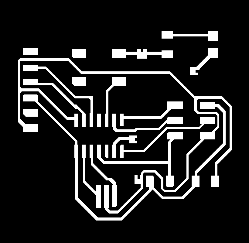
In any case, after many many different attempts of routing the board, I'm getting a little frustrated. This is a part which is surprisingly complicated. Specifically, I see why the button and led were added - this makes the design not straightforward, and requires significant effort to get right.
After changing the spacings and making about 20 different configurations and attempts at routing it all, I came to the conclusion that it won't be possible to route all of these paths properly on just one layer. I'm going to need to add some wires, to go over existing connections, in order to finish establishing all of the necessary routes.
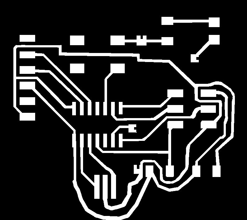
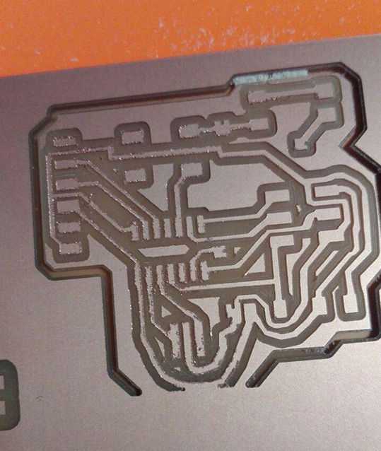
So in the end, this is what I came up with:
.jpg)
The square bits are going to have a wire soldered to them connecting all three of them together. That will complete the circuit. And then I noticed that my flat 6pin is not rotated correctly, and the actual pins themselves will end up facing inside. I think. I assume. It made my cry inside a little, but I reoriented stuff around again and routed them all again…
So after about 20 attempts more and some more internal silent crying, I arrived at this solution:
.jpg)
With only one skip connection, complying with the milling machine's settings and minimum spacing requirements, and relatively compact. FINALLY!!!!! I am too happy now T_T
And now: File > Export > Image, with 1000DPI resolution and Monochrome.
.jpg)
Um, the parts are still there. I need just the circuit.
Ah okay, it's in the email:
.jpg)
.jpg)
.jpg)
.jpg)
.jpg)
.jpg)
After following this, and making some adjustments in Photoshop (just cropping an image, and making the shape of the board itself), I have these two:
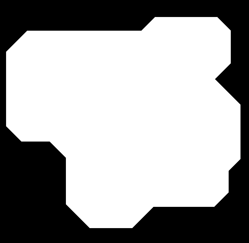
And of course the schematics which do show each item's configuration.
.jpg)
.jpg)
Next step is to get this actually printed, then soldered correctly.
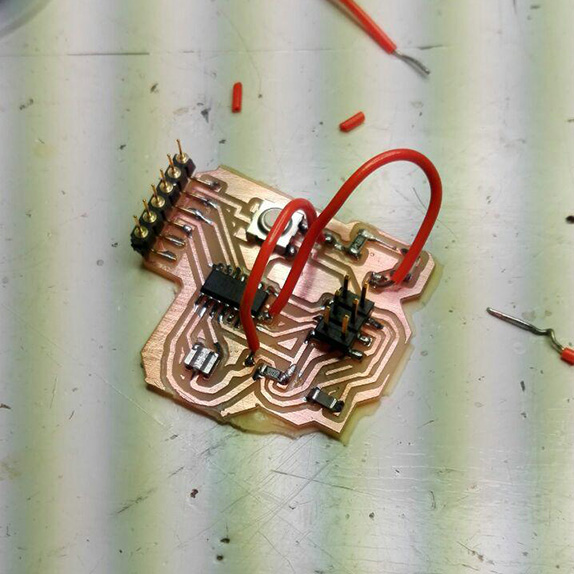
Quick note - I actually made a small modification to the board design, because in the original schematic Emma sent there was a connection between the route coming out of the button to the route coming out of the resonator, so I just made a small change there - added two rectangles to solder another wire.
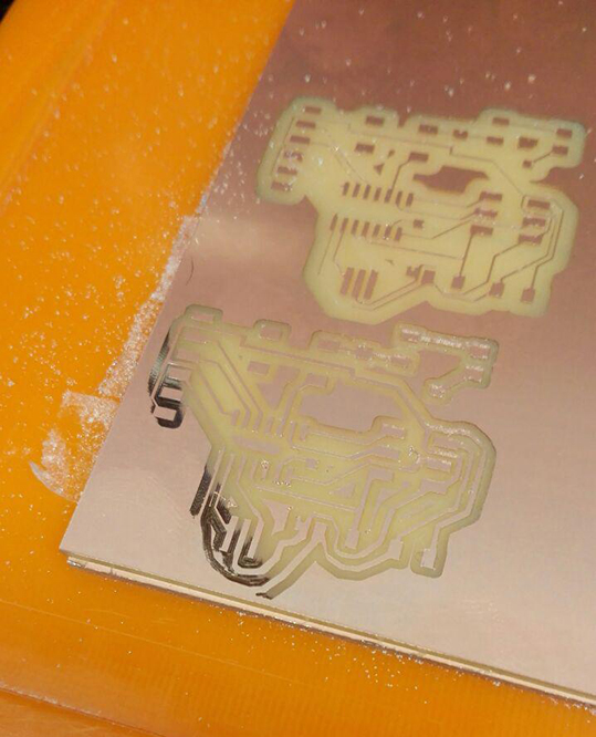
MILLING THE BOARD
I milled the board several times at the lab. The first time, my result was this:
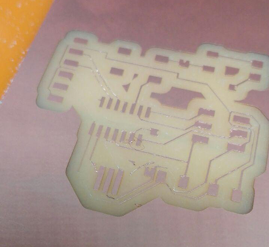
It came out really bad, with multiple traces being simply ripped off the board. I made a few modifications to the schematic, manually, to make thicker traces out of suspicion that the reason it failed is because they're too thin.
Milling that, I got a funny mess up in the process, with the bottom half of the board no longer being milled and instead being completely polished:
Perpahs the bit got dulled, so I change bits and went ahead to mill it again, one last time:
Unfortunately, this attempt has also failed, some of the traces were coming loose / being grinded somehow, and the actual board itself was not even fully cut out - the 1/32 bit did not go through the whole way.
I could not attempt it again as I had to leave for work, but during the regional review session, Emma, our local instructor, suggested that my last circuit actually does not look bad, and just needs a little cleaning. In the break she demonstrated how this is done, and so I did just that, and it actually did end up making the circuit completely usable.
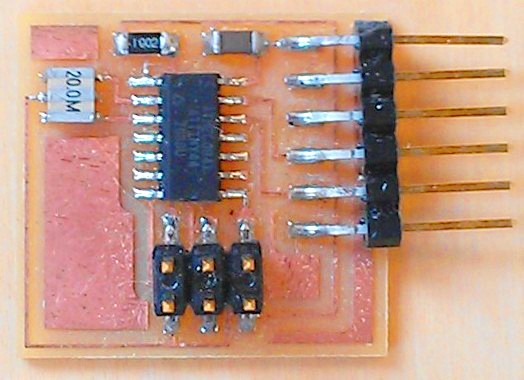
What more - I took to a screwdriver, a hammer, and expertly knocked the whole circuit board out.
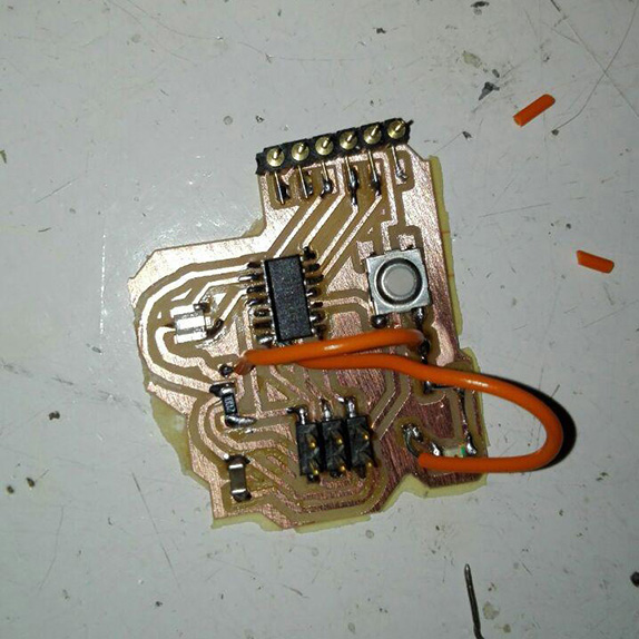
I then utilized the remaining time of the break to solder all the different components together:
And I tested the circuits with a multimeter to make sure I don't have any short circuiting or any issues:
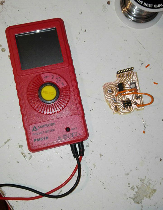
It all looks good. Looks like I'm done! :D Who'd have thunk it, what a wonderful day this is turning out to be :)
Eagle Schematic and Board files:
SchematicBoard
Back home