FABACADEMY
Electronics Design
Welcome to my week 7
Electronics Design
Learning Outcomes:
ACHIEVEMENTS THIS WEEK:
Electronic Components
Assignment:
Redraw the echo hello-world board add (at least) a button and LED (with current-limiting resistor)
Brief:
Electronics is the discipline dealing with the development and application of devices and systems involving the flow of electrons in a vacuum, in gaseous media, and in semiconductors. Electronics deals with electrical circuits that involve active electrical components such as vacuum tubes, transistors, diodes, integrated circuits, optoelectronics, and sensors, associated passive electrical components, and interconnection technologies. Commonly, electronic devices contain circuitry consisting primarily or exclusively of active semiconductors supplemented with passive elements; such a circuit is described as an electronic circuit.
Process:
- For this week’s group assginment - visit here.
Firstly, going through resources given by fab academy about the components, methods and softwares.
Then we had a brief inroduction given by our instructor about the week's assignment.
Using Eagle which i had installed beforeU can Download the software Here
I followed the following steps:
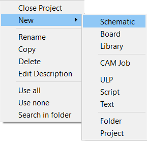
1. Open Eagle and login if your using first time.
2. Make a new project
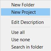
3. Choose Schematic
4. Select Option USE to choose library.
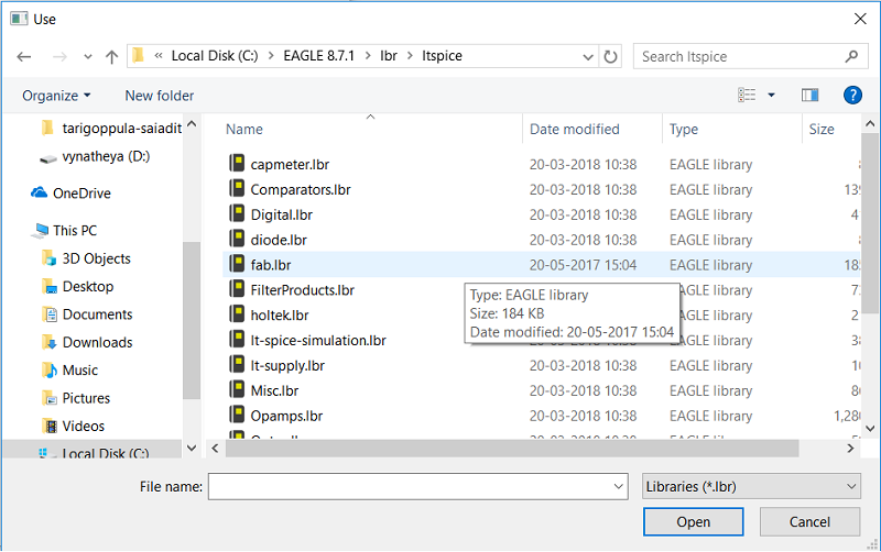
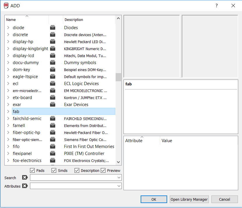
I started by importing FAB LIBRARY to Eagle. You can download the library from here Instruction to install the library can be found here.
Open library manager
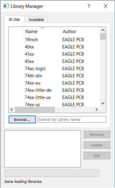
Select fab.lbr
Search Library in Add components
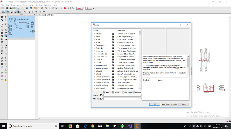
5. You will see the fab library there, you can start adding components.
6.I started by adding ATtiny 45, placed it on the board, Press esc and choose next. in that way i added all the components.........
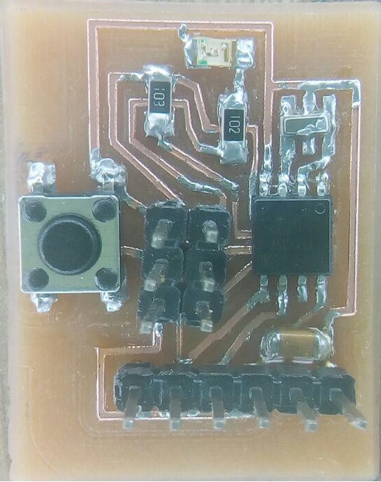
The following Components were used for this board:
A) Resistors
B) Capicitors - 1 uf
C) IC Attiny 45
D) Connectors 2x3 and 6x1
E) Resonator
F) LED
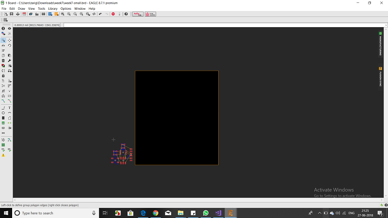
Board Layout
Now to convert this schematic to Board layout we need to click on this Icon over the tool bar SCH BRD
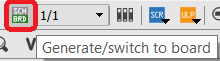
click on the board icon
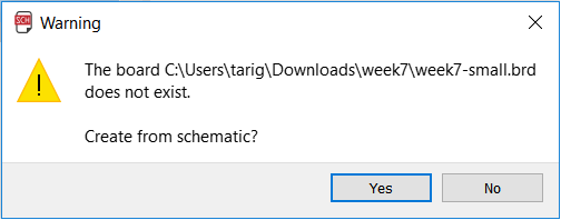
Now a new window would appear which would be like this click yes....
Now in this window the dark Black area within the orange boundary is our main work area or we may say this is the area which is going to be printed we need to put all the components within this area. This operation can be done using simple drag and drop.
Now I started to set the design rules and net list to make sure everything is within the limits of SRM 20.
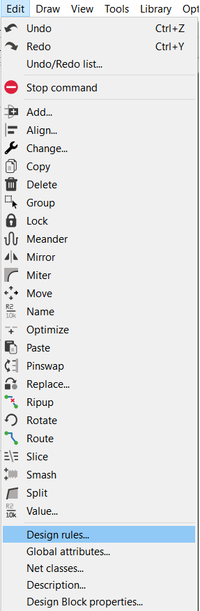
Go to Edit and then Design Rules
Open Design Rules
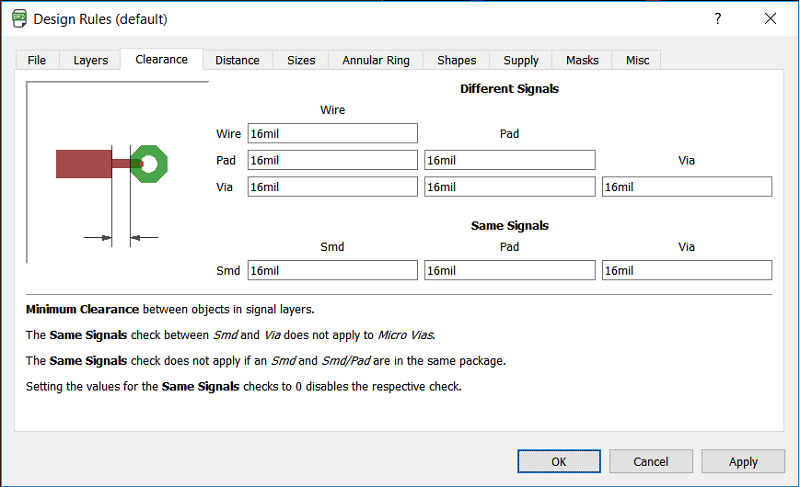
Clearance
Now 1st thing we need to set is the clearance, In this window we would be defining all the clearances, either its betweeen two tracks or between tracks and pads etc etc ....., In our lab we would be using 1/64 bit so the trace would be about 16mils.
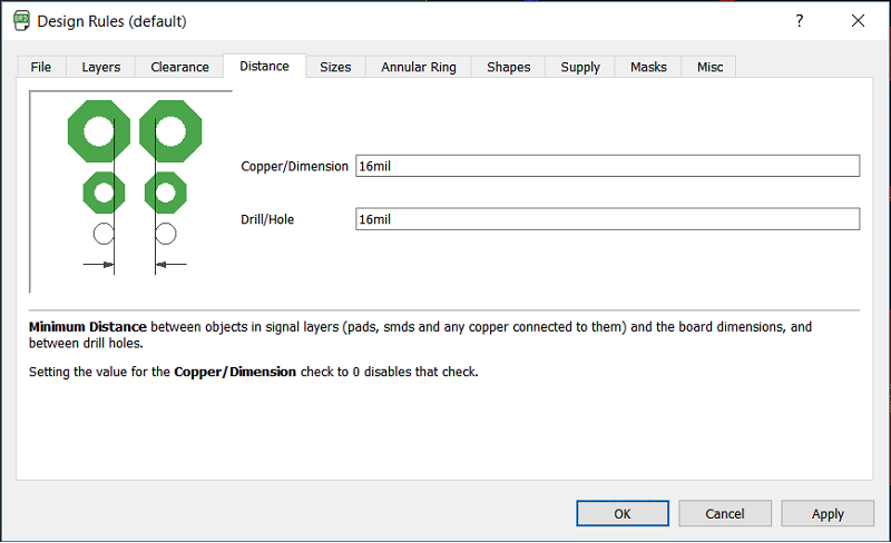
Distance
Corresponding to 16mils track I changed its default value by 16mils
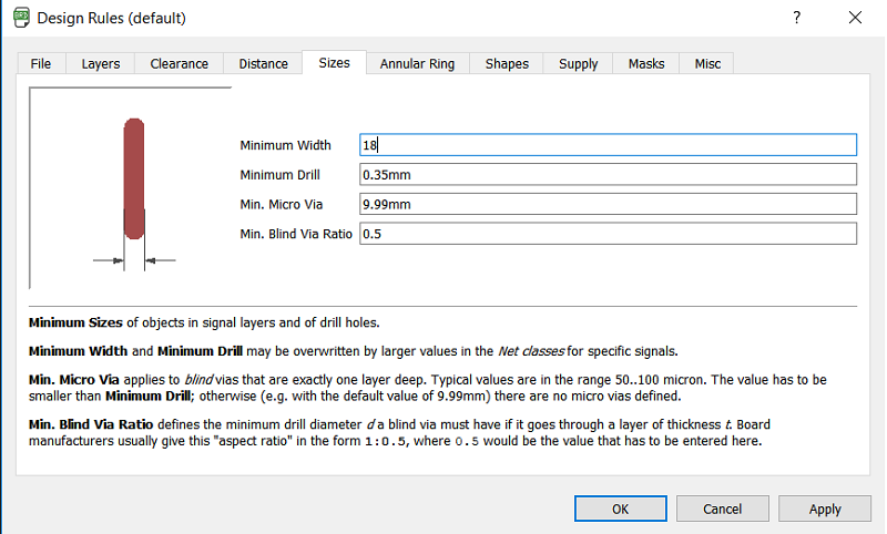
Size
To be on the safe side I increased the size of the track to 18mils as 16mils was the minimum track width that my tool could have milled.
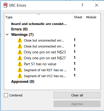
After setting all the design parameters, we need to run a ERC- Electronic Rule Checker
Click on the ERC Icon on buttom right side of the tool bar
The rule checker shows some warning which are due to me, not giving values to some components. we can approve them all and now we are ready to start Routing.

After setting all the rules we can move ahead with routing it may be noticed that there are airwires which seems to make the board look complicated I used ratnest to clear out extra air wires and then I moved ahead for auto routing..
I tried doing auto routing but I am not satisfied with it so after some time I re routed the design and then am satisfied with it .
Switch and LED Connections.
Switch :- My switch is connected to the pin 3 of attiny 45 and the other one is connected to the GND
LED :- My LED is connected to the pin 7 of attiny 45 and the other one is connected to the GND
This was the design which I made before given below.
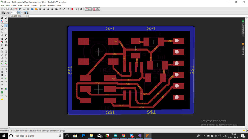
This was the re design which I made after given below.
Download .sch and .brd file here...
It is also important for u to name and components and valus it name it so that it is help full to soldering and to share u r design
For more info about reading Schematic & Name Designators and Valueshere