WEEK 7: ELECTRONICS DESIGN
Day 4
I’m incredibly behind this week.
I missed the classes that explained what we were doing do I can barely understand what is going on.
I’m still trying to understand what we did the last time we did electronics.
So, apparently we’re just connecting a microcontroller to a led and a button and we need to program it so that the button turns the led on and off.
We’ll see how that goes.
Day 8
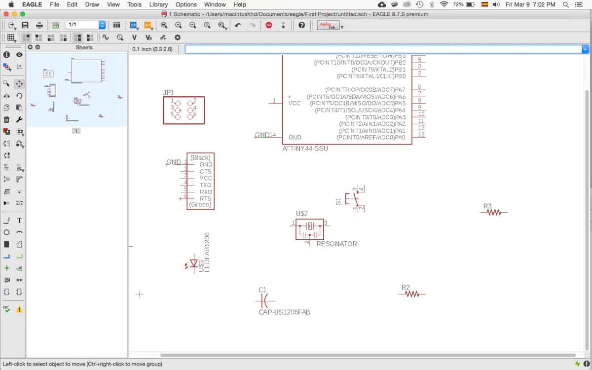
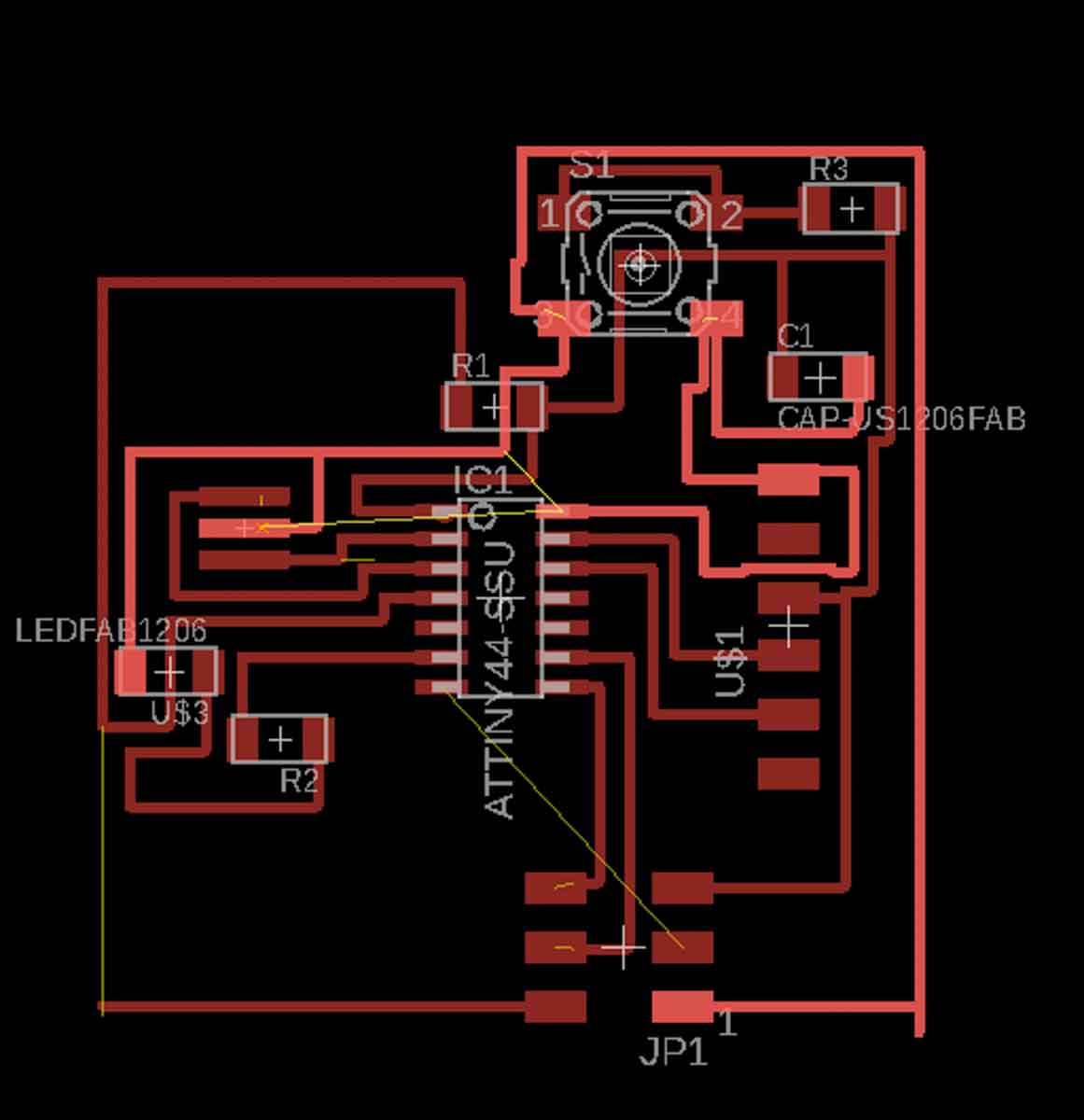
So, I’m behind, that much is already obvious, but after some youtube tutorials I think I may be able to basically redraw Neil’s board and add a button and an led.
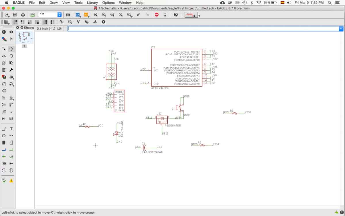
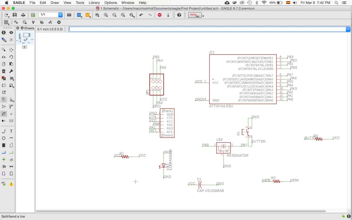
Alright, so, as far as I can gather, I’ll be using a program called Eagle, that is used to scheme and design circuit boards. There were other options but this program is free and compatible
The program itself is really interesting seeing as it has a set of libraries consisting of electronic parts, and as you select them, the Schematic part of the program appears. And so I had to include the fab library to my Eagle library so I could use the precise parts we have available at the lab, in the program. I did this by copying this file to the lbr folder created into my computer inside Eagle’s directory.
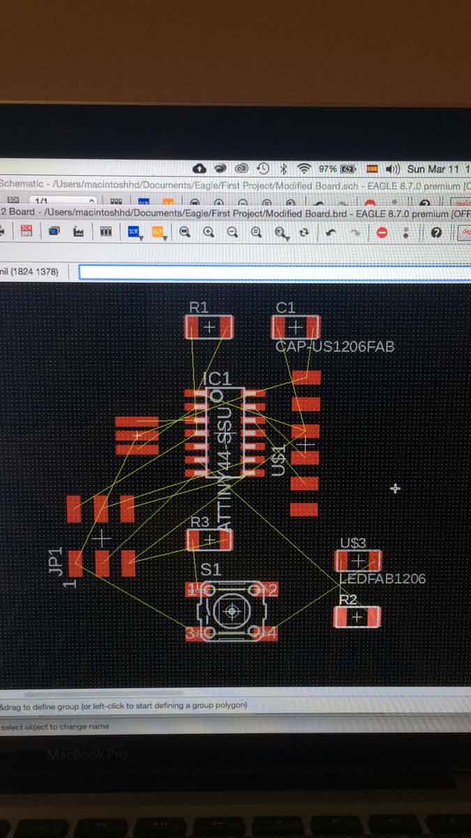
Once you’ve selected your parts and made the connections between those parts, you can import those parts and connections into the Board setting of the program and draw the actual shape of those connections.
What’s particularly useful here is that it allows you to set parameters such as the width of those drawn connections, it alerts you when you’re drawing too close to the components (depending on the setting you’ve put in) and most important, all the components in each library are in real scale, so is you select the right component, when in Board mode, they’ll be the pads drawn there will be the correct size and in millimeters from the get go.
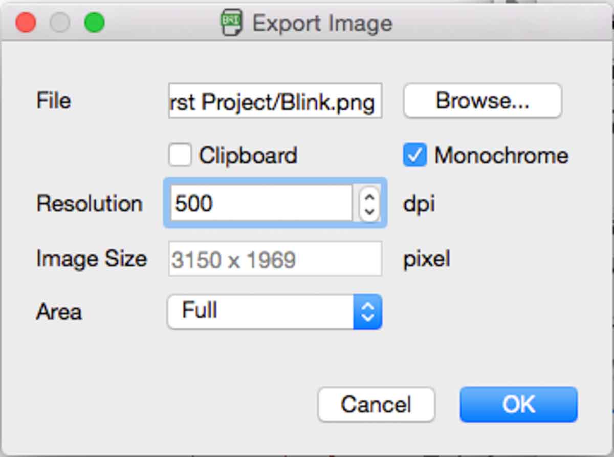
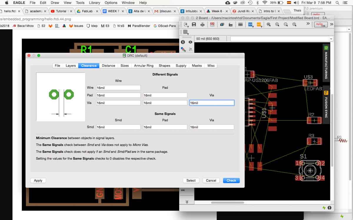
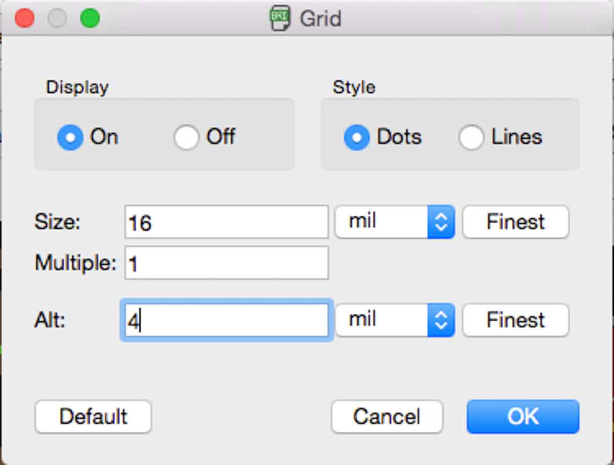
For our purposes this is fundamental, given that one of the parameters we need to set is the minimum width of between any given pad or trace (16mm, which is the size of the milling tracing tool) and for people like me, who really don’t know what the components are, what they do or what they look like, it’s great that the program already knows the correct dimensions of each one.
Day 9
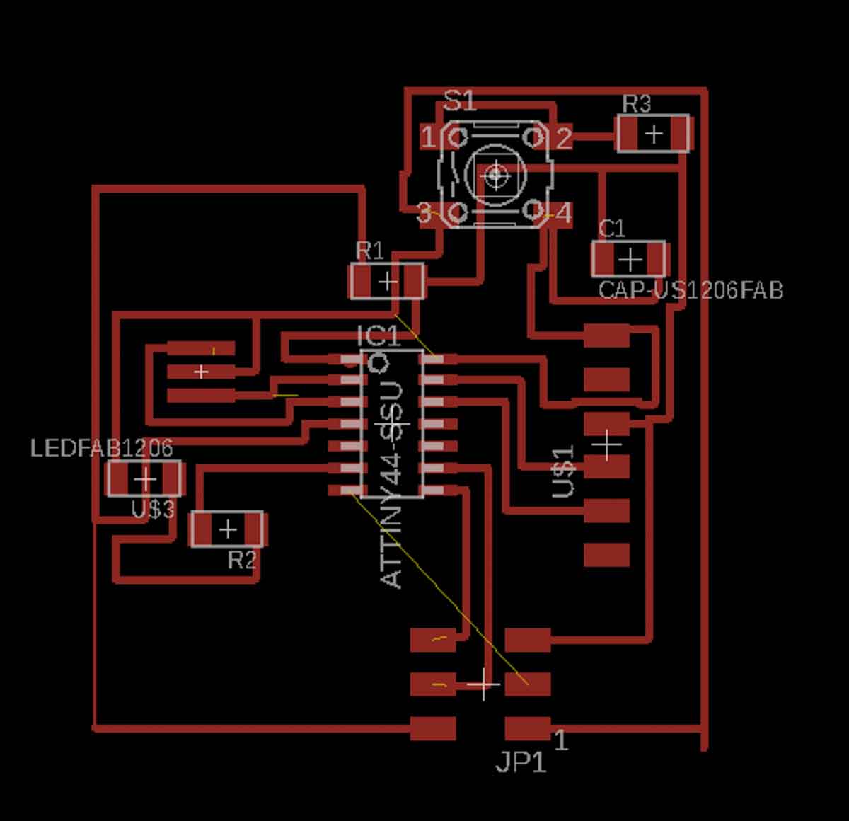
It was challenging to make the connections by myself. I spent hours trying to figure out how to redraw the paths that were already established but the VCC always clashed with the GND. I decided to try to replicate the design provided exactly, seeing as I found no other way to modify it and make all the desired connections.
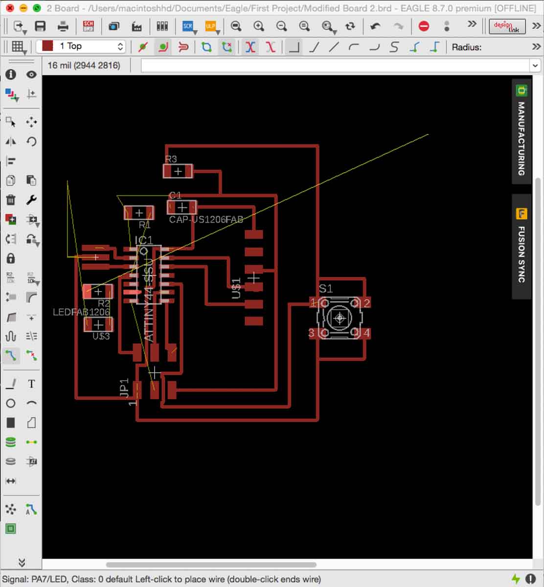
The milling process didn’t go as well as the first time. The PCB separated from the base during the milling process and it completely ruined it.
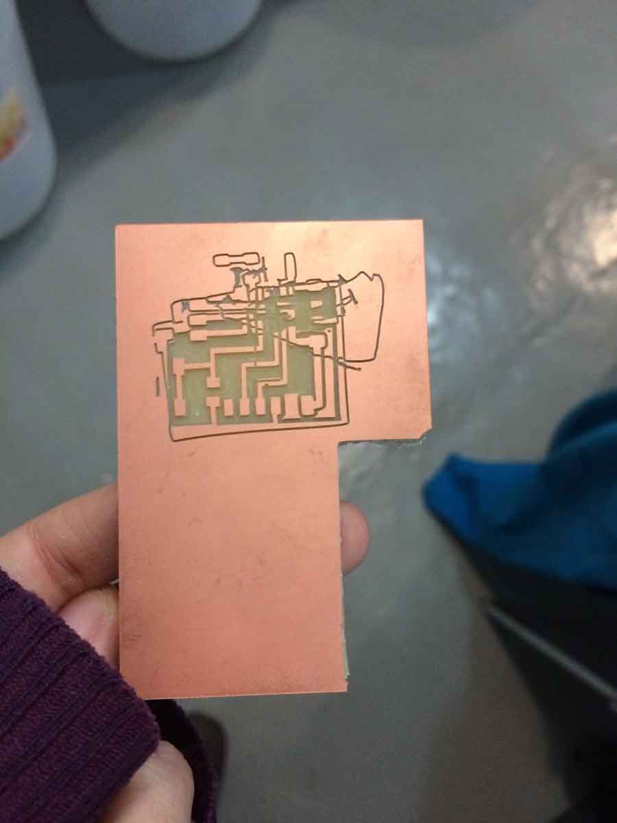
The second attempt was better but I decided to do it a third time because I accidentally broke one of the lines when I was manually cleaning the excess material from the board and I wasn’t convinced with the improvised fix.
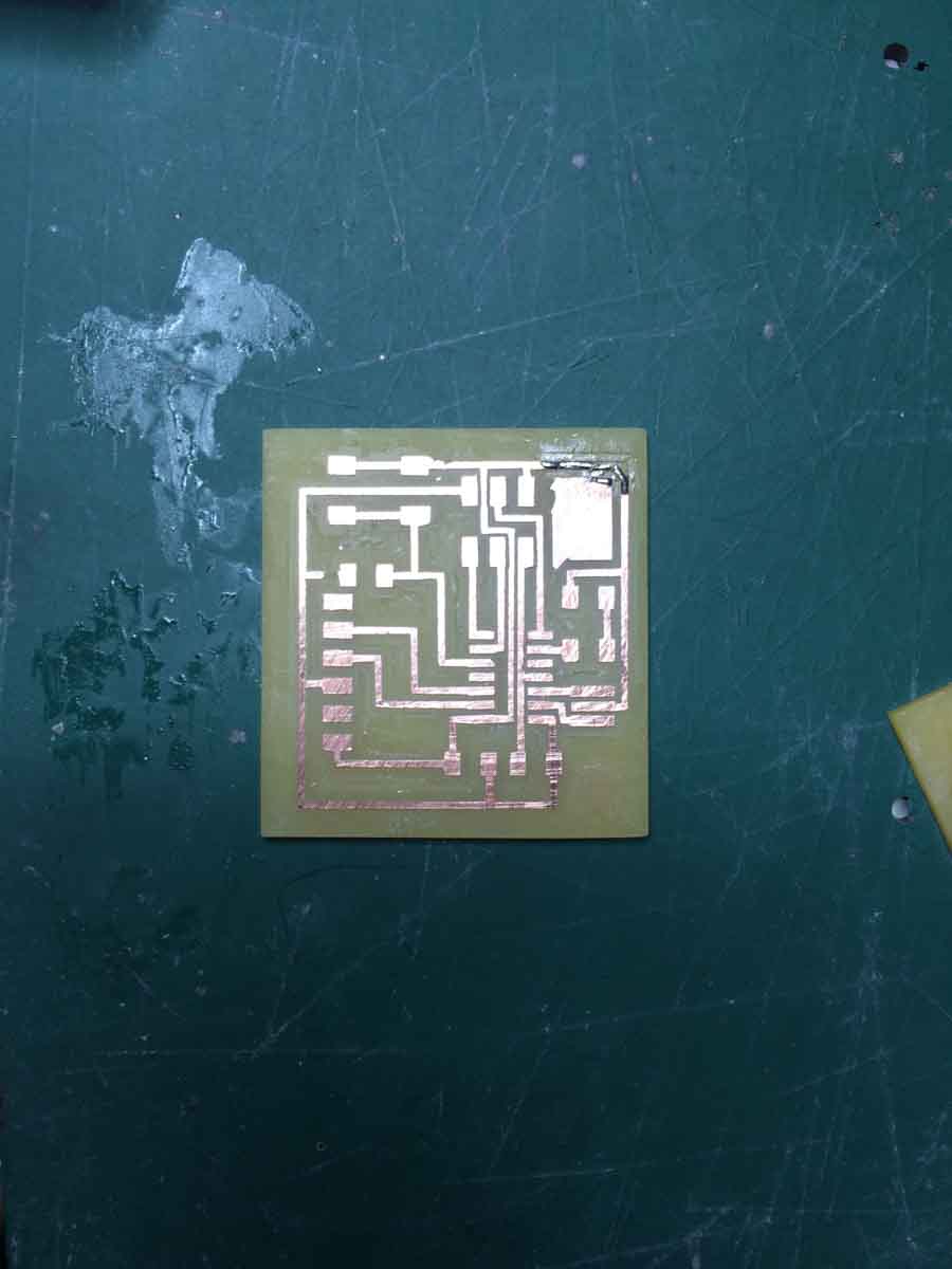
Once I got the milling done I had to look for the parts and solder them.
This time the soldering was easier and more enjoyable.
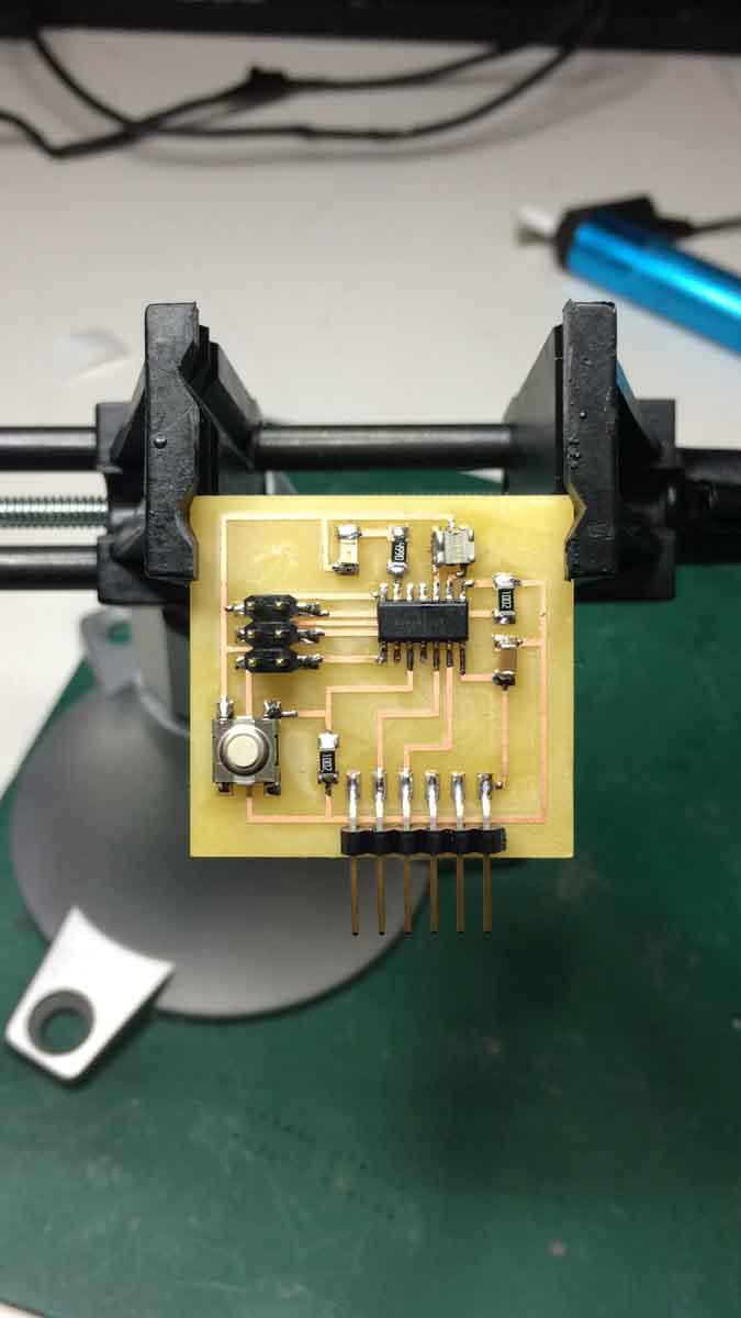
In order to verify continuity and lack of shortcuts, I used a multimeter before plugging the board to the computer. The multimeter has two probes (red + black) and they have different ends, alligators-shaped tweezers on each end. To check the continuity, there is a mode where we can check if two lines are connected and the multimeter will beep in this case if you turn on the volume setting and so, you check each trace, from pin to pin or pin to pad, as it were, to verify that all connections are working. It’s not too much, when using a microcontrollers with many pins, to check if there isn’t a short underneath the microcontroller, in case any soldering or error during the milling, accidentally connected two traces that shouldn’t be connected.
The files can be downloaded here and here.