Schnyder - Electronics Design: Creating an Anthropomorphic
Circuit Layout
This week we had to design and make a circuit board that used the
ATTiny 84 IC and included an LED and a button. I used the EAGLE
program with the FAB library installed to lay out circuits and do
board design.
I focused on the circuits first. I had no experience with EAGLE
so initially I focused on duplicating the basic circuit layout for
the ATTiny 84. I learned from this that the physical connections
made in the circuit design affected how the rat's nest of
connection in the board layout was assembled. I used a lot of
truncated connections in the circuit layout and relied on
consistently naming to establish a connection between discrete
parts. When it came to the board design the connections were in
place but crossed components or appeared in a different order than
I would have expected. I also experimented with the autorouter
where I got the idea to use vias in my design. The blank stock we
had used for the FabISP had copper on both sides and I decided to
take advantage of that. So I decided to use vias to get to the
backside (the ground plane).
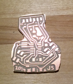
Once I had the basic circuit laid out and a basic board designed
(using a rectangular layout) I went back to the circuit designer
and added components: a 4-pin header, 2 LEDs and related resistor,
and a momentary switch. With these new components, I started to
have fun with the layout and got to a point where I saw a face in
the circuit. Seizing the opportunity, I decided to make a bust.
The purple lines represent traces on layer 16, the backside of the
board. Since only ground went to the backside, I decided that I
could keep the solid copper surface.
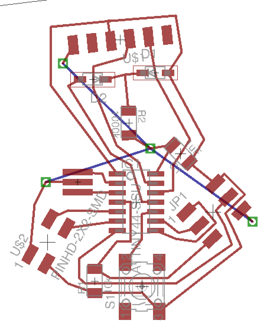
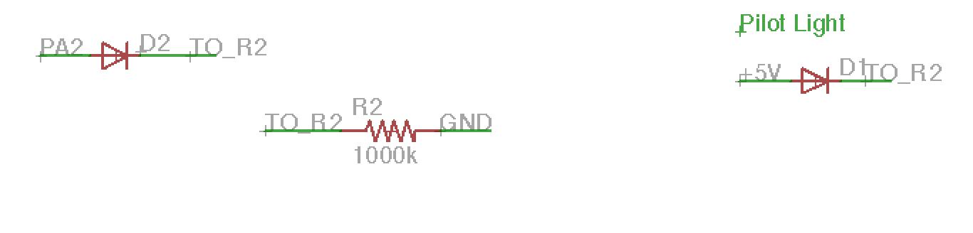
I made a decision to reduce the numbers of parts by one--both LEDs
share the same resistor. One LED indicates whether the six-pin
header has a plug with the correct orientation (the Pilot Light_.
The other LED indicates when PA2 is set to high.
Another constraint was to get the resonator as close to the IC as
possible. Excessive trace lengths apparently can cause timing issues
although I don't know how long the traces have to be before there is
an issue.
The next step was to check tolerances of the space between pads and
tracers assuming that the milling machine head was about 16 mil. I
first did this at home and didn't understand that the program marks
the problem areas. I thought that I was seeing some sort of bizarre
bug. I was corrected and then I spent a little bit of time
correcting the problems. I had about 8-10 adjustments to make.
During the layout I had used a 15mil snap guide. For the
adjustments, I reduced the snap grid size to gain better fine
tuning.
I turned off the bottom layer and exported the traces and vias to a
png file. I set the output resolution for this file to 1000 dpi. I
then exported only the traces to use this as the starting point for
the cutout file.
I finished these graphics in The Gimp. I imported both files as
layers in a single document. By varying the opacity of the top
layer, I could see the underlying traces and it was easy to draw the
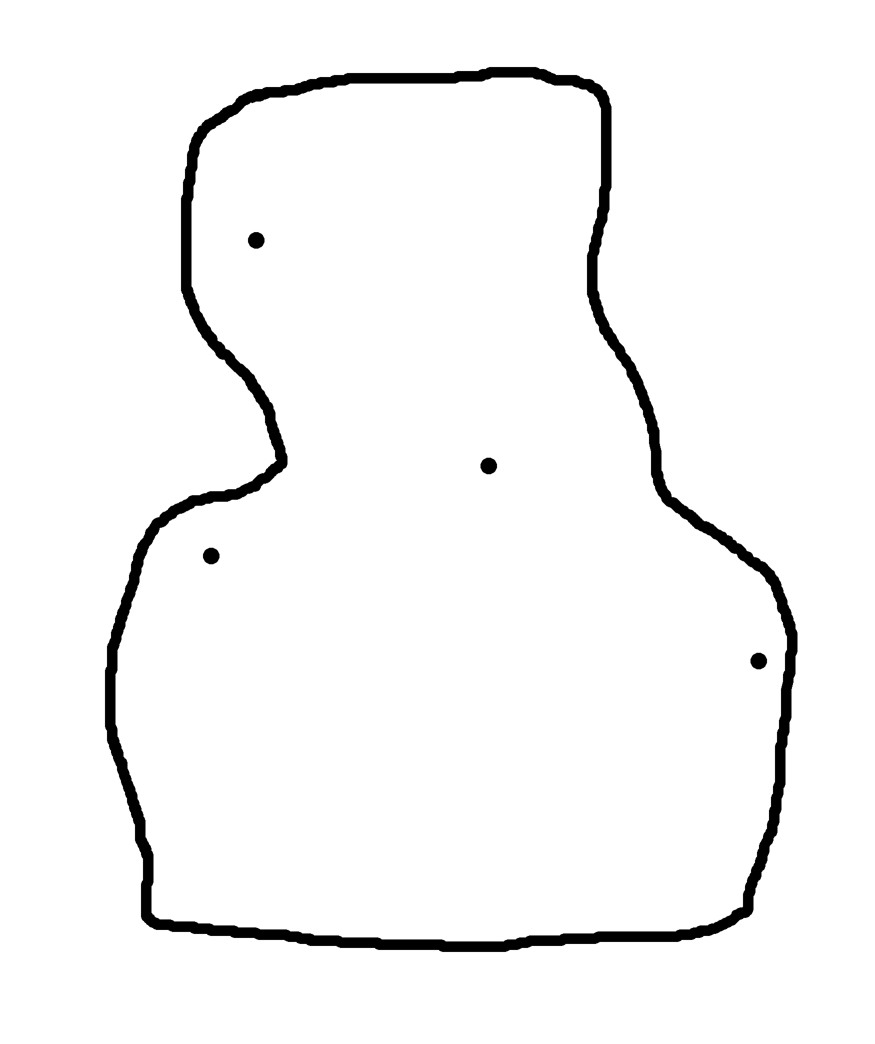
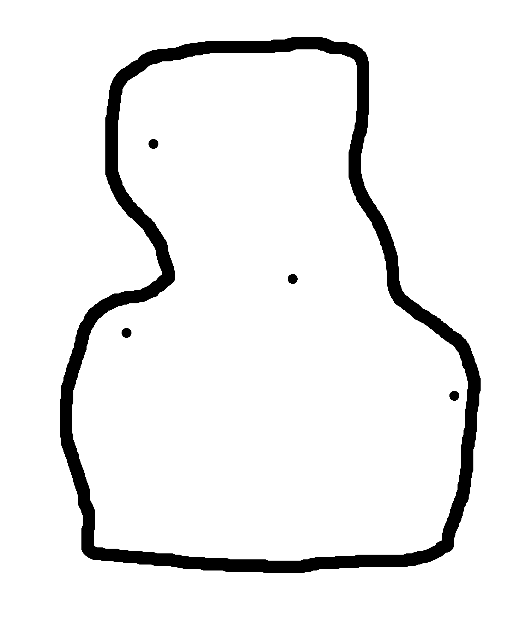
cutout line and add my initials and the year. The cutout line that I
drew ended up being too thin for the Fab program and Modela. When I
imported the png and made the path, the window with the tool path
was blank. I did try to adjust the diameter of the cutter and
eventually saw the lines around 0.60 mm, but when I sent it the
Modela acted as if it was in a raster-like mode. Upon closer
inspection of the path, it was not contiguous.
I also forgot to invert the trace image. This caused a brief delay
in milling when the path did not look right for the traces. It is an
easy fix in The Gimp.
I canceled the job, thickened the line and reloaded it. This time
there were no issues. The two images below show the before and after
cutout files.
Here is the board.
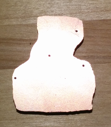
I shared the FR1 blank with two other students and we spent an
excessive amount of time trying to get the cutter to go all the way
through the board. We first tried it with the default values for the
1/32 cutter in the Fab module. When that didn't cut through the
board, we measured the thickness of the board (0.16 mm) and set the
bottom depth to 0.18 mm. We made sure the the tool bit was zeroed
just below the surface of the copper. It still didn't cut all the
way through. We then went to 0.22 mm and that worked. I didn't have
as much trouble with my cutout and I think that the cause is that
the other areas of the board was set over a part of the sacrificial
layer that was pretty chewed up, so the board might have been
flexing.