Additional Images and Videos of this project are on my tumblr blog:
part1 part2 part3 part4
Our assignment this week was a continuation of the processes we covered in week 5 when we milled and “stuffed” our own circuit boards to build a micro controller called the fabISP.
This time around our assignment required us to actually design the circuit pattern to be milled out rather than using a pre-existing design downloaded from the web.
Well, kind of. Actually we did something halfway in between. We were given a pre-existing circuit design and we were tasked with modifying the design to include an LED and a button. The name of the board we were starting from is the “Hello Echo” board, and my understanding is that we’ll be using it in future assignments alongside the fabISP.
At the moment, though, I have no idea what it does or how it is supposed to work.
All the images I took of this project are from the assembly (or “stuffing”) phase, but the majority of the steps are done on the computer using a design program called Eagle.
The first step in the project, besides downloading and installing software, was to download the schematic for the Hello Echo board and import it into the EAGLE software.
EAGLE, which stands for Easily Applicable Graphical Layout Editor, is software which allows you to download libraries of manufactured electronics parts and arrange them in a schematic like pieces of a puzzle. The program will connect all the components to one another according to your specifications, and then with a little manipulation it can generate the layout of the milled out connections.
Basically you arrange all of your components on a virtual board, then establish the connections between them, and because the program already has the specifications of all the parts you’re using, it will generate the correct shapes in the correct sizes to define mounting points for all of the components on the board. Then you move the mounting points around to your liking, and draw all of the connections between them. At this point you can generate an image file which can be output to a CNC milling machine to carve out the copper plates which make your board.
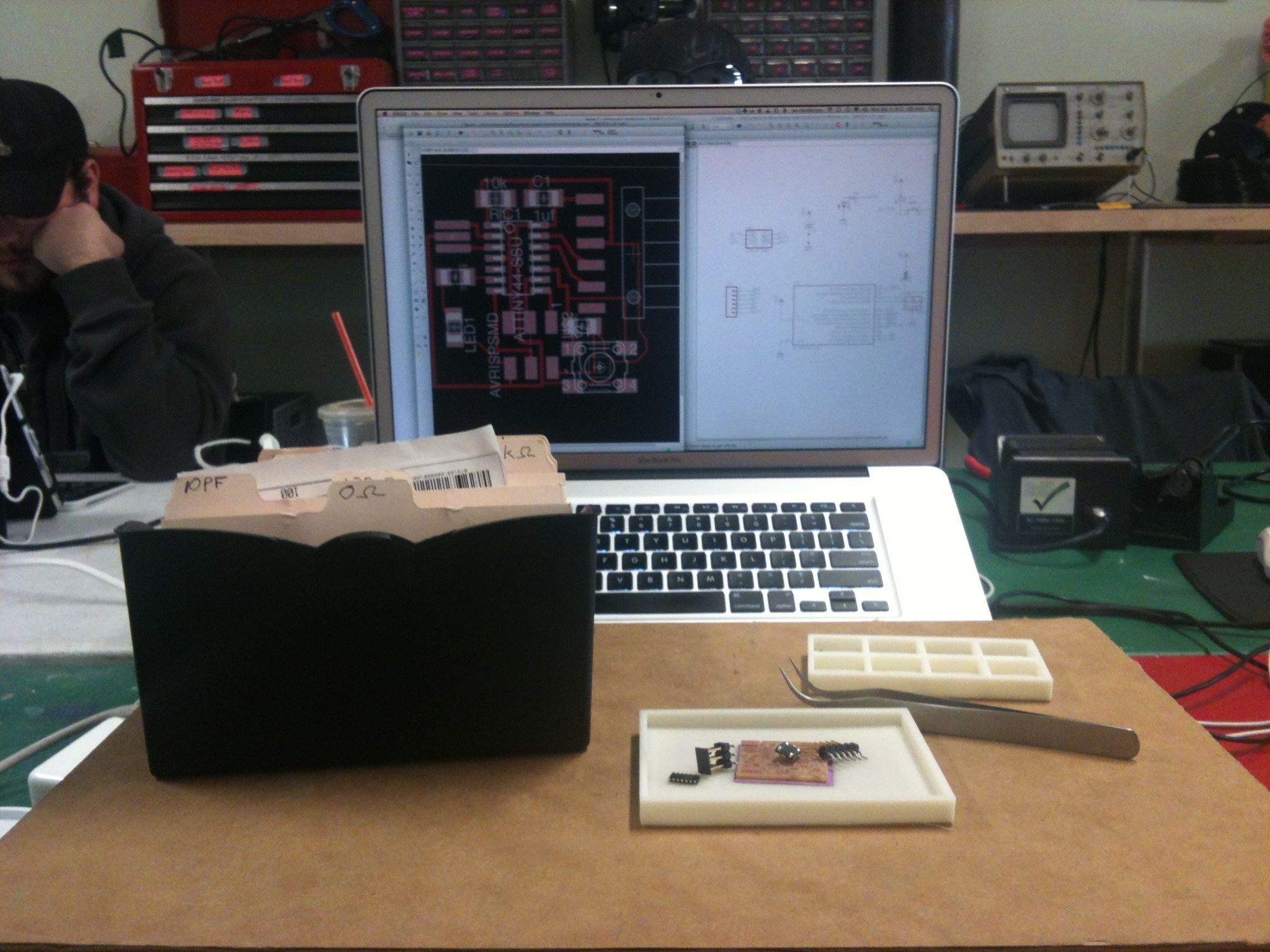
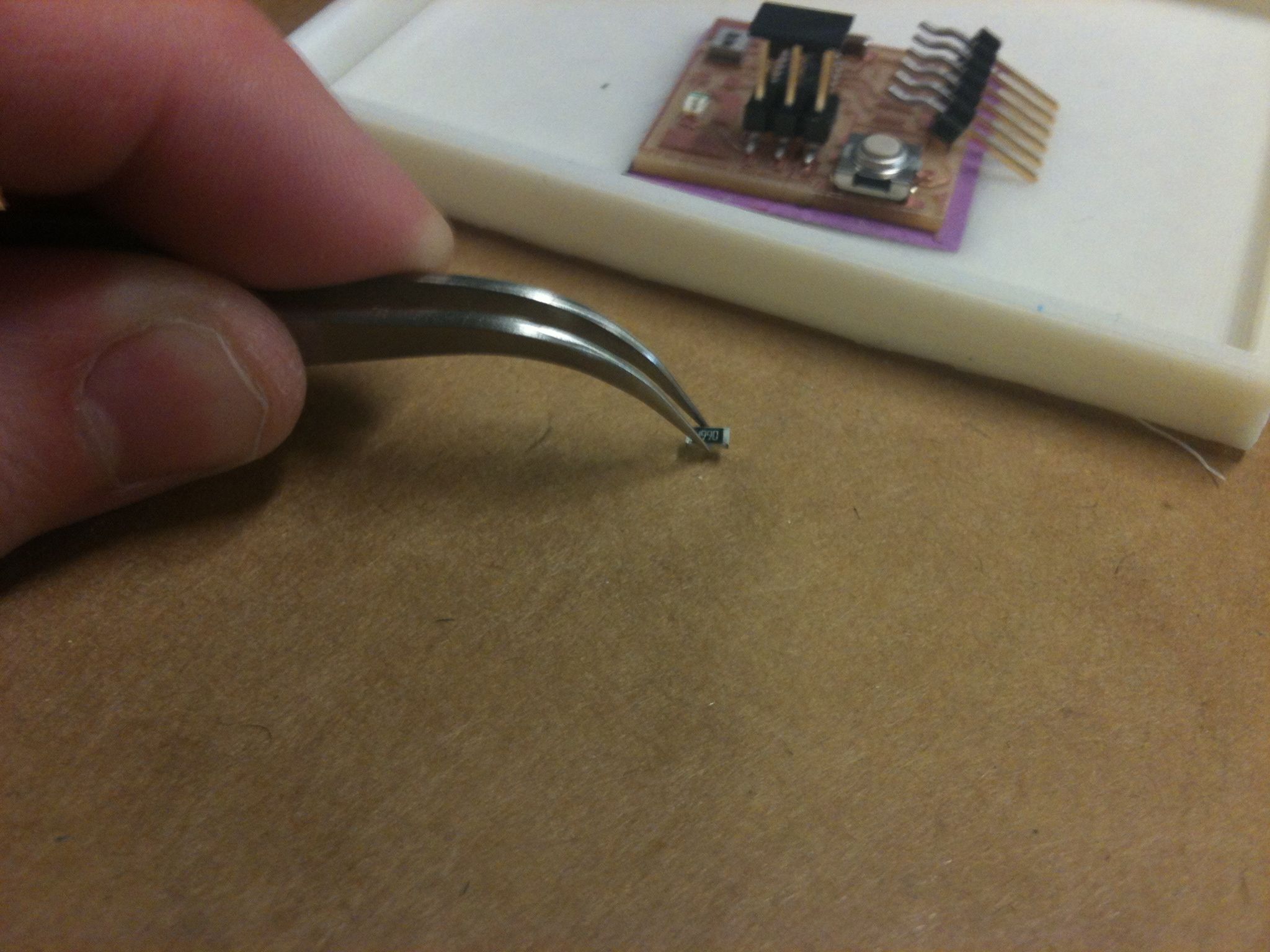
Once the design is finalized, you mill it out in the same way as the fabISP was done, and then it’s just a matter of soldering all the components in place. This time around it was a bit trickier since I couldn’t go the whole “match colors and shapes” route since there was no example board or “correct” schematic to copy, which meant I had to riffle through these folders full of components and kind-of-sort-of figure out how to read the labels.
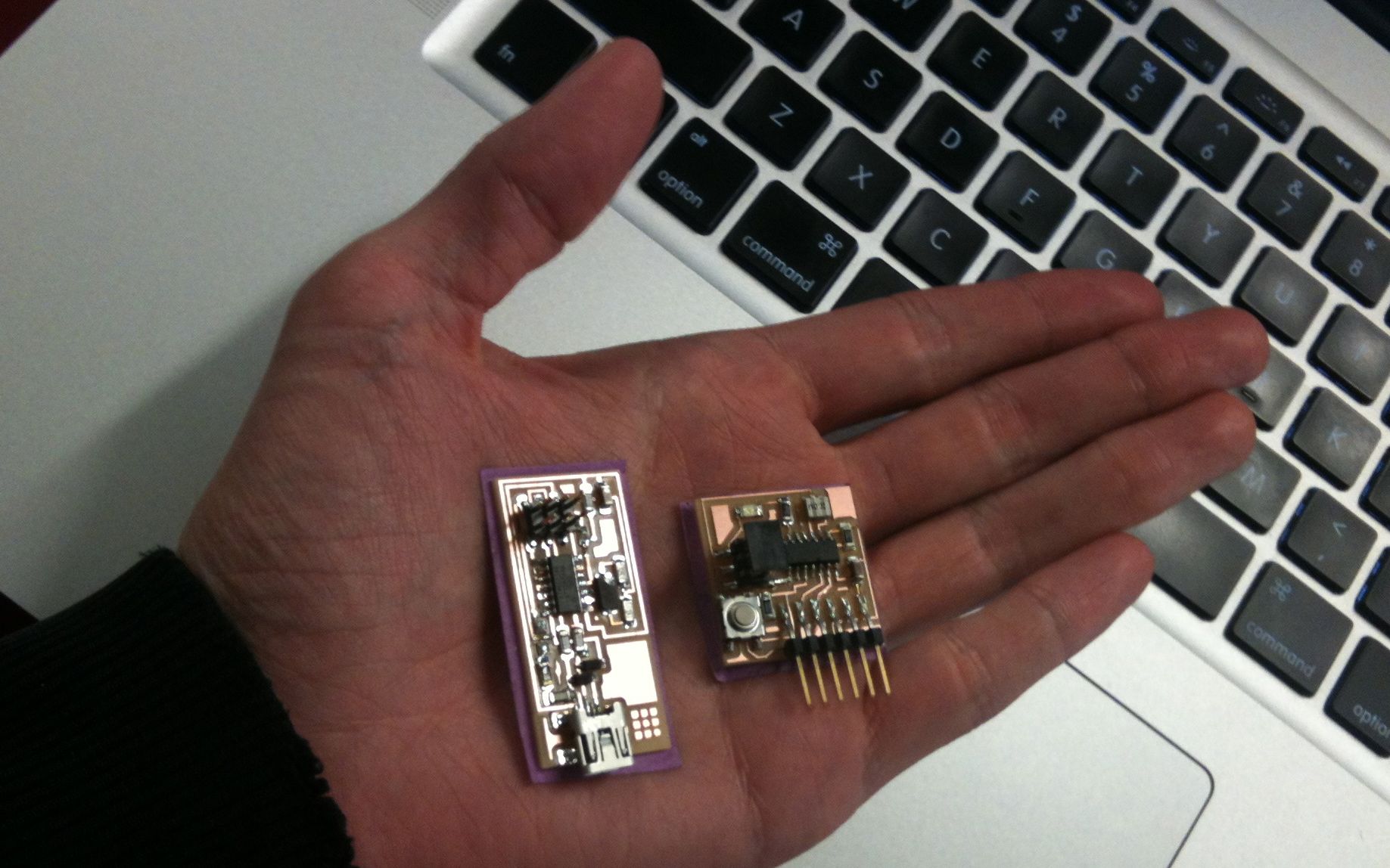
Once the board is milled and the components are picked out, it’s a fairly straightforward soldering job. In the final picture you can see both of the completed boards side by side: fabISP and HelloEcho:
May 28 2012 13:36
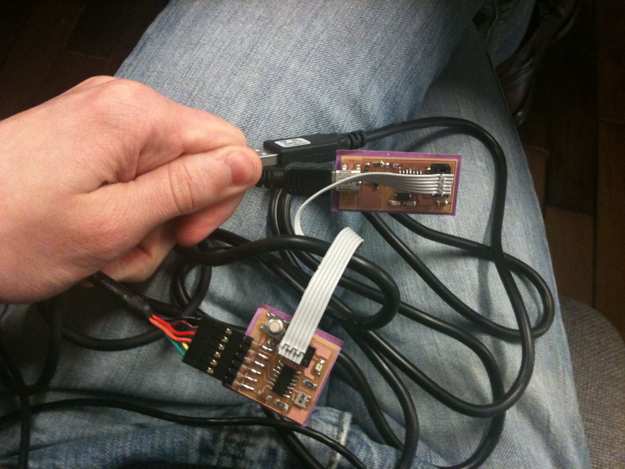
Snap-off FabISP
I decided it would be nice to have a FabISP which plugs directly into my USB port without the need for an additional cable, so I downloaded the plans from this student's website: http://fab.cba.mit.edu/classes/863.11/people/valentin.heun/2.htm
I followed the information as closely as I could, though I didn't have any 18pF capacitors and substituted with 33pF capacitors instead. Also, the info sheet didn't indicate any values for the zener-diodes, so I used 3.3v since that's what we used for the original FabISP. Hopefully it'll still work.