This week assigment is about electronic design, for this we'll have to modify a microcontroller board adding to the original design a button and a led.
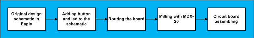
The picture shows the the work flow for the assigment, with the reverse engenieering to the board design to get the original schematic, then modifying it, folowing routing, milling and assembling the circuit board.
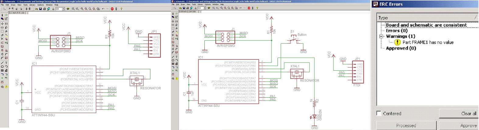
The schematics with the original design and the requested modification. The ERC verification help me to verify that the schematic was ok, just a warning but no errors.
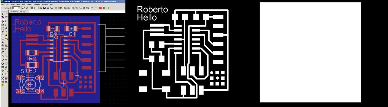
The board layout and the *.png files for top (traces) and bottom (cut profile) sides of the board.
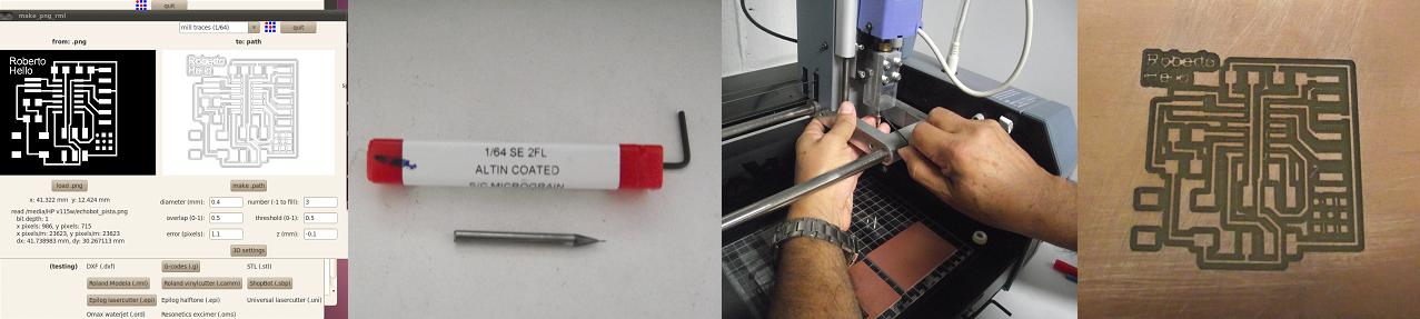
This time milling was easier than the ISP board, because the circuit tracks were not to close
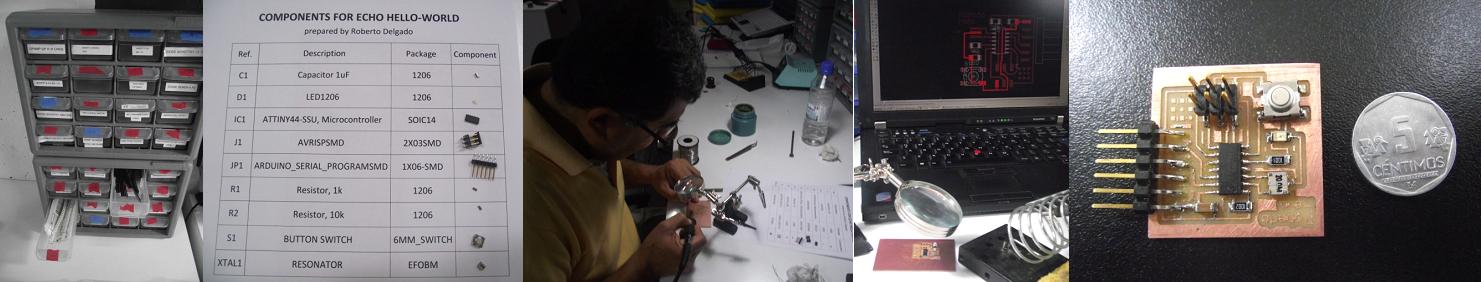
Pick up of the components, preparing for assembling and the assembled board. I used the Eagle layout image of my computer to higlight the traces for identifiying it.
This assigment shows the great help offered by CAD tools like Eagle in electronic design.