Home > Final Project
So I Finally decided against building a complete cyclonic filtration system. The more I learn about this, the more I find that i still need to learn to pull this one off.
So my final project is going to be:
The Fabscope is a device that fablabs are able to make using their existing inventory (mostly) (see fabinventory 2012).
Shortlist of what has been acomplished:
Basically there are 2 parts to the scope. The hardware and the firmware. First i'll be explaining the hardware design considerations. Next is the firmware.
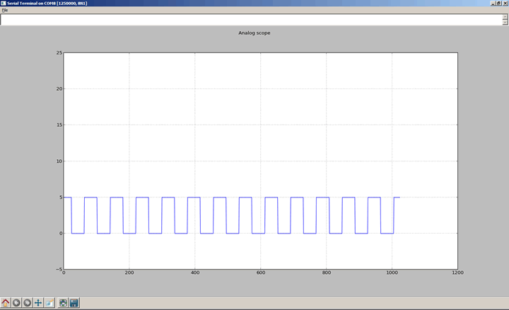
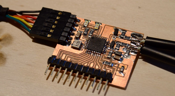
The system is based around an AtMega328p, which is connected to a computer where the sensed data is visualised.
The mega328 contains an ADC (analog to digital converter) which can be set to use an external reference voltage. A 3.3v zender diode (which actually puts the voltage at 2.7V) is used to get a good stable reference voltage as opposed to using the (noisy) 5V apllied by the computer.
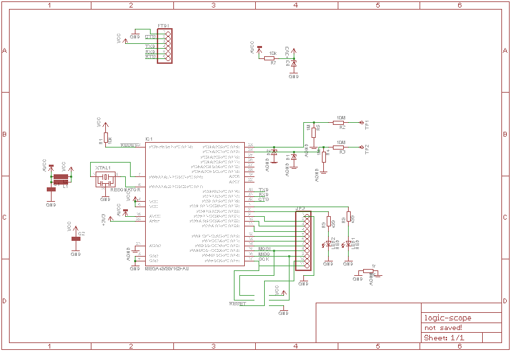
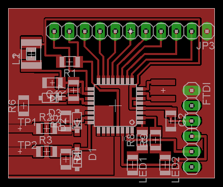
I dicided to implement this right away. It makes a lot of sense to extend the range from 0-5 to 0-50V. But the main reason i did this is so i can lower the reference voltage on the ADC while still getting a decent measurement range. For the first design i used 10M/1Mohm resistors. But i soon found out that i had a problem with my adc when using such high ohmage resistors.
The ADC needs to charge it's 'sample and hold' capacitor. This needs to draw a certain amount of current from the system we're measuring. Too big of a resistor between the ADC and the target signal means the capacitor does not get charged fast enough, and thus giving an erroneous reading.
So my next design will use an op-amp as voltage follower to get a powerful enugh signal into the arduino, but have almost no drain on the input signal.
The firmware was written in processing (arduino) but i later skipped using most of the libraries.
AnalogInOutSerial
Baudrate calculator http://www.wormfood.net/avrbaudcalc.php?postbitrate=9600&postclock=20&bit_rate_table=on
Maximum baud rate achievable with a 20 Mhz resonator and usign 2x speedup would be 2.5 Mbit/s, however. The ftdi chip used for receiving this data is only capable of receiving 3Mbit or 2Mbit, there is no devisor for in-between values.
So a 16 Mhz crystal would be a better choise, as that will allow us to communicate at 2Mbit (using Double Speed UART)
So using FabInventory, the highest Baud rate achievable would be 1.25Mbit/sec.
Fastest reading of digital port state would be to take the 8-bits form a single port (saves time on combining results from 2 registers in a single register). Unfourtunately this impossible on the Mega328 cpu. The 8 bits are coming from Port D 6/7 and Port B 0-5.
Why use buffering?
Basically storing in SRam can be done faster than that the result can be communicated to the computer.
Drawback of this is that while the buffer is communicated to the computer, no measurements are done. (a bit like the 'retrace' in analog scopes)
So how much time does it take to get the result into a register ready to store/send?
    IN portD to register 1                (1 cycle)
    AND to keep just bits 6-7             (1 cycle)
    IN portB to register 2                (1 cycle)
    AND to keep just bits 0-5             (1 cycle)
    AND to combine reg1 with reg2         (1 cycle)
So 5 cycles to get the 8-bits into the register.
Using the USART at the maximum possible speed, (UBBR0 = 0) standard async mode takes 16 cycles to transfer a single bit. Operating it at double speed (bit U2X0 set to 1) takes 8 cycles per bit, and using it in Syncronous mode would take it further down to 2 cycles per bit. The FTDI cable we're using doesn't support Synchronous mode, and is actually only rated up to 1Mbit/s for RS232 mode. I've succesfully used 1.25MBit/s and people have even pushed it to 1.6Mbit/s with arduino's.
And then i found out about the bit bang possibilities of the FTDI cable we're using. There are even some pyhon interfaces available to the ftdi D2XX drivers. Further improvements would be made when using this bit-bang modus (see (1) (2) and (3).
So in standard mode, it would take 160 cycles to send a byte (1 start, 8 data, 1 stop. So 10 in total with 16 cycles per byte). Synchronous mode would bring that down to 20.
The advantage is that, as the sending is done in hardware, it runs in parallel with getting the results from the pin/ADC-registers
    ST store register in SRAM (post inc)                            (2 cycles)
    CP compare low byte of SRAM pointer to top value                (1 cycle)
    BRNE branch back to saving next value if compare is false       (2 if false, 1 is true)
    CP compare high byte of SRAM pointer to top value               (1 cycle)
    BRNE branch back to saving next value if compare is false       (2 if false, 1 is true)
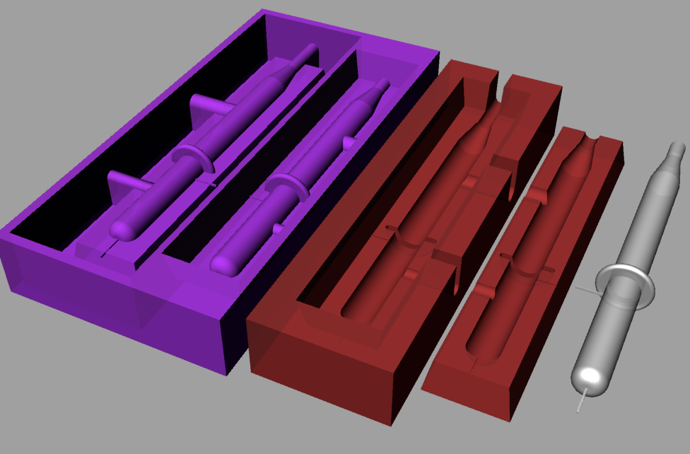
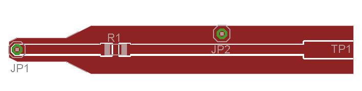
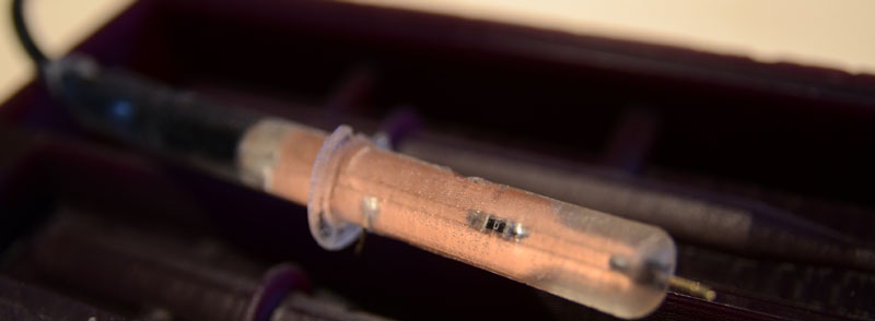
This design allowed me to experiment with various in-probe components.
The first probe hast just a 0-ohm resistor on R1 to directly relay the signals to the adc-port on the AtMega. (featured on the top of this page.
JP1 is the probe point (a single pin from a normal SMT jumper
JP2 is the connection for a ground-clip.
TP1 is the location where the connecting wire to the scope attaches.
For connectors i've chosen the tulip-connectors. The wire connecting the probe to the scope is flexible 75Ohm microphone cable.
Design-file: probe.3dm (rhino 3d file)
The software currently only displays the samples as it receives them from the scope.
The software is written in Python (2.7) uses wx-widgets, numpy, matplotlib and pyserial.
On Probes:
http://www.syscompdesign.com/AppNotes/probes.pdf
http://www.cromwell-intl.com/radio/probes.html
Microcontroller:
http://www.atmel.com/Images/doc8161.pdf